3 memory map/register definition, 1 register overview, 3 memory map/register definition -7 – Motorola ColdFire MCF5281 User Manual
Page 507: 1 register overview -7
General Purpose I/O Module
Freescale Semiconductor
26-7
Chapter 14, “Signal Descriptions
” for more detailed descriptions of these pins. The function of
the pins (primary function, GPIO, etc.) is determined by the various ports registers and the mode of
operation. Refer to
for detailed descriptions of pin functions.
26.3
Memory Map/Register Definition
26.3.1
Register Overview
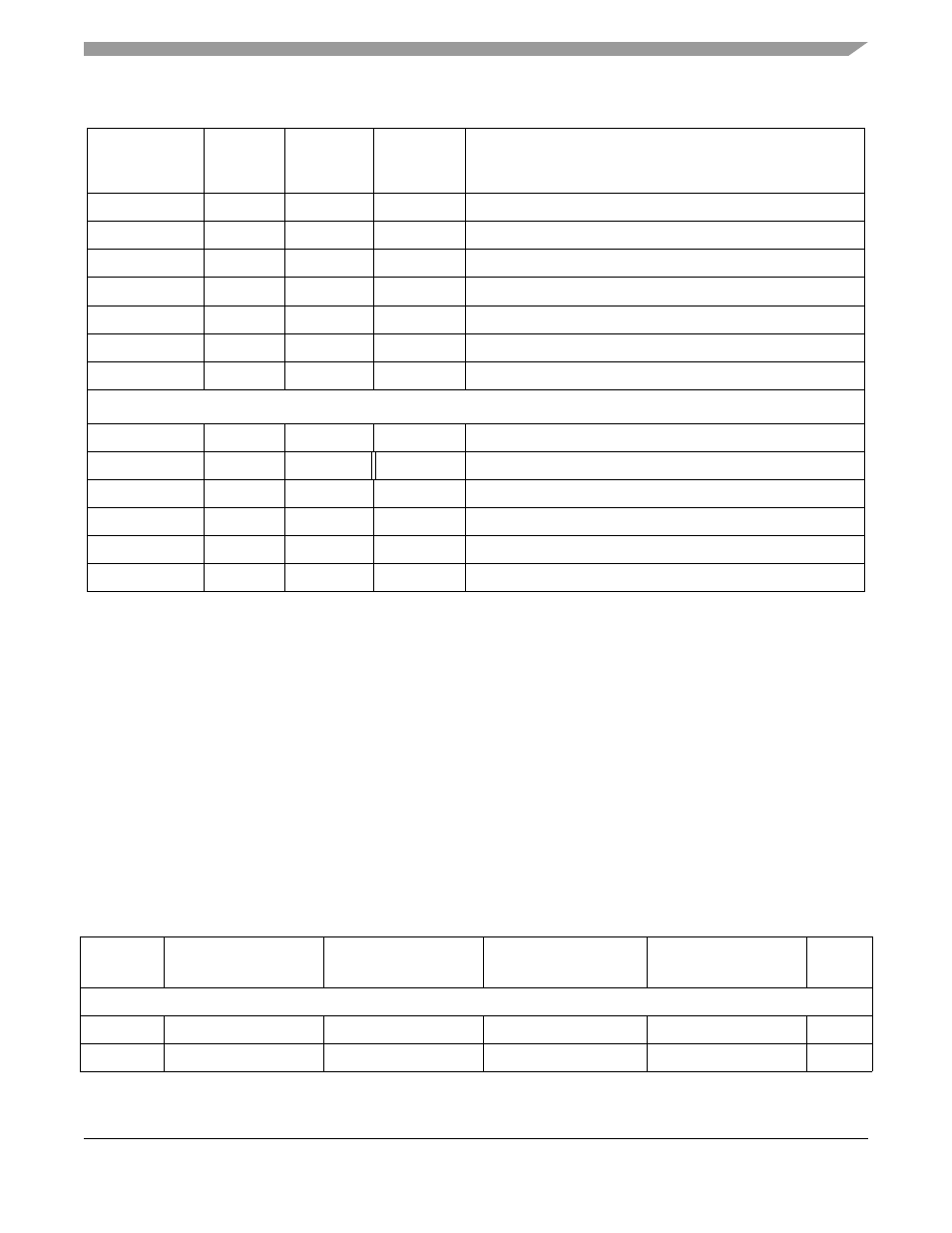
summarizes all the registers in the ports address space.
ECRS
PEH[0]
—
—
Ethernet carrier receive sense / PEH[0]
ETXD[3:1]
PEL[7:5]
—
—
Ethernet transmit data / Port EL[7:5]
ETXER
PEL[4]
—
—
Ethernet transmit error / Port EL[4]
ERXD[3:1]
PEL[3:1]
—
—
Ethernet receive data [3:1] / Port EL[3:1]
ERXER
PEL[0]
—
—
Ethernet receive error / Port EL[0]
EMDIO
PAS[5]
URXD2
—
Ethernet management data control / Port AS[5] / URXD2
EMDC
PAS[4]
UTXD2
—
Ethernet management data clock / Port AS[4] / UTXD2
The following signals apply to MCF5214 and MCF5216 only
PEL[0]
—
—
—
Port EL[0]
PAS[4]
UTXD[2]
—
—
Port AS[4] / UTXD2
PEL[7:5]
—
—
—
Port EL[7:5]
PEL[4]
—
—
—
Port EL[4]
PEL[3:1]
—
—
—
Port EL[3:1]
PAS[5]
URXD2
—
—
Port AS[5] / URXD2
1
The primary functionality of a pin is not necessarily the default function of the pin after reset. Pins that have muxed GPIO
functionality will default to GPIO inputs.
2
Function available in master mode only
3
Pins not actually part of Port Module, but included here for complete listing of available I/O ports. See separate section for
description of this port.
Table 26-2. Ports Module Memory Map
IPSBAR +
Offset
31–24
23–16
15–8
7–0
Access
1
Port Output Data Registers
0x10_0000
PORTA
PORTB
PORTC
PORTD
S/U
0x10_0004
PORTE
PORTF
PORTG
PORTH
S/U
Table 26-1. Ports External Signals (continued)
Primary
Function
(Pin Name)
1
GPIO
(Default
Function)
Alternate
Function 1
Alternate
Function 2
Description
MCF5282 and MCF5216 ColdFire Microcontroller User’s Manual, Rev. 3