3 dram controller mask registers (dmr0/dmr1), 3 dram controller mask registers (dmr0/dmr1) -8, 0) [p. 15-8 – Motorola ColdFire MCF5281 User Manual
Page 280: 1) [p. 15-8

Synchronous DRAM Controller Module
15-8
Freescale Semiconductor
15.2.2.3
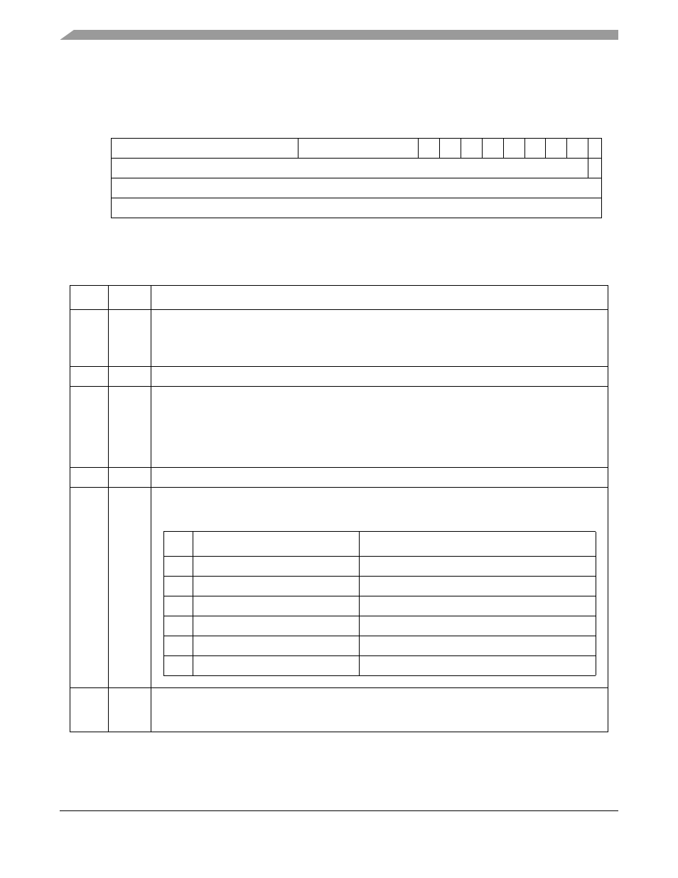
DRAM Controller Mask Registers (DMR0/DMR1)
The DMRn,
, includes mask bits for the base address and for address attributes.
describes DMRn fields.
31
18 17
9
8
7
6
5
4
3
2
1
0
Field
BAM
—
WP —
C/I AM SC SD UC UD V
Reset
Uninitialized
0
R/W
R/W
Addr
IPSBAR + 0x04C (DMR0), 0x054 (DMR1)
Figure 15-4. DRAM Controller Mask Registers (DMRn)
Table 15-6. DMRn Field Descriptions
Bits
Name
Description
31–18
BAM Base
address
mask.
Masks the associated DACRn[BA]. Lets the DRAM controller connect to various
DRAM sizes. Mask bits need not be contiguous (see
.”)
0 The associated address bit is used in decoding the DRAM hit to a memory block.
1 The associated address bit is not used in the DRAM hit decode.
17–9
—
Reserved, should be cleared.
8
WP
Write protect. Determines whether the associated block of DRAM is write protected.
0 Allow write accesses
1 Ignore write accesses. The DRAM controller ignores write accesses to the memory block and an
address exception occurs. Write accesses to a write-protected DRAM region are compared in the
chip select module for a hit. If no hit occurs, an external bus cycle is generated. If this external bus
cycle is not acknowledged, an access exception occurs.
7
—
Reserved, should be cleared.
6–1
AMx
Address modifier masks. Determine which accesses can occur in a given DRAM block.
0 Allow access type to hit in DRAM
1 Do not allow access type to hit in DRAM
Bit
Associated Access Type
Access Definition
C/I
CPU space/interrupt acknowledge
MOVEC instruction or interrupt acknowledge cycle
AM
Alternate master
DMA master
SC
Supervisor code
Any supervisor-only instruction access
SD
Supervisor data
Any data fetched during the instruction access
UC
User code
Any user instruction
UD
User data
Any user data
0
V
Valid. Cleared at reset to ensure that the DRAM block is not erroneously decoded.
0 Do not decode DRAM accesses.
1 Registers controlling the DRAM block are initialized; DRAM accesses can be decoded.
MCF5282 and MCF5216 ColdFire Microcontroller User’s Manual, Rev. 3
