Motorola ColdFire MCF5281 User Manual
Page 256
Signal Descriptions
14-16
Freescale Semiconductor
J14
DTIN0
PTD1
UCTS1/
UCTS0
Timer 0 in
I/O
—
J13
DTOUT0
PTD0
UCTS1/
UCTS0
Timer 0 out
I/O
—
Queued Analog-to-Digital Converter (QADC)
T3
AN0
PQB0
ANW
Analog channel 0
I/O
—
R2
AN1
PQB1
ANX
Analog channel 1
I/O
—
T2
AN2
PQB2
ANY
Analog channel 2
I/O
—
R1
AN3
PQB3
ANZ
Analog channel 3
I/O
—
R4
AN52
PQA0
MA0
Analog channel 52
I/O
—
T4
AN53
PQA1
MA1
Analog channel 53
I/O
—
P3
AN55
PQA3
ETRIG1
Analog channel 55
I/O
—
R3
AN56
PQA4
ETRIG2
Analog channel 56
I/O
—
P4
VRH
—
—
High analog reference
I
—
T5
VRL
—
—
Low analog reference
I
—
Debug and JTAG Test Port Control
R9
JTAG_EN
—
—
JTAG Enable
I
—
P9
DSCLK
TRST
—
Debug clock / TAP reset
I
Yes
7
T9
TCLK
—
—
TAP clock
I
Yes
P10
BKPT
TMS
—
Breakpoint/TAP test mode select
I
Yes
R10
DSI
TDI
—
Debug data in / TAP data in
I
Yes
T10
DSO
TDO
—
Debug data out / TAP data out
O
—
C12:D12:A13:B13
DDATA[3:0]
PDD[7:4]
—
Debug data
I/O
—
C13:A14:B14:A15
PST[3:0]
PDD[3:0]
—
Processor status data
I/O
—
Test
N10
TEST
—
Test mode pin
I
—
Power Supplies
R5
VDDA
—
—
Analog positive supply
I
—
P5:T1
VSSA
—
—
Analog ground
I
—
P2
VDDH
—
—
ESD positive supply
I
—
N8
VDDPLL
—
—
PLL positive supply
I
—
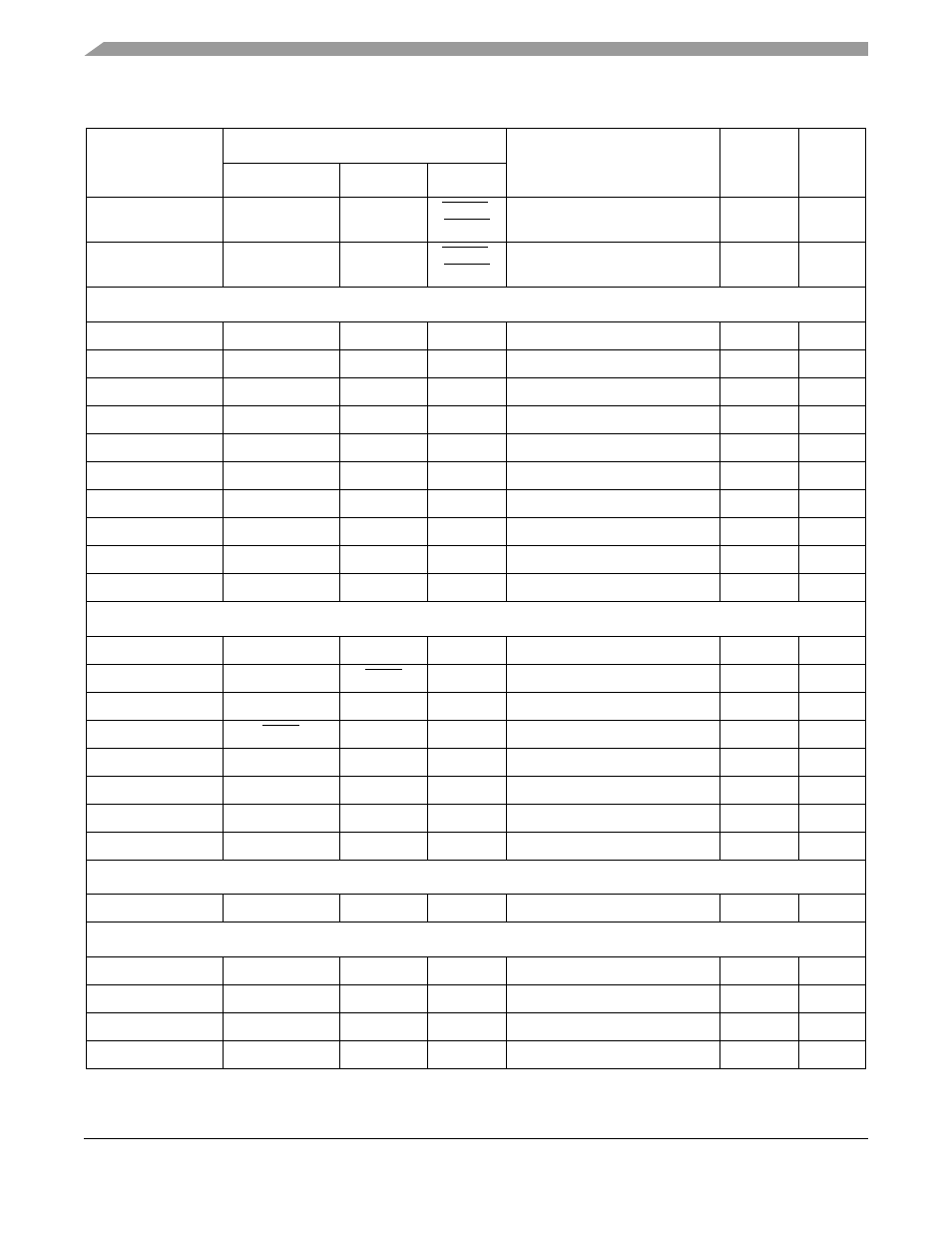
Table 14-3. MCF5282 Signals and Pin Numbers Sorted by Function (continued)
MAPBGA Pin
Pin Functions
Description
Primary
I/O
Internal
Pull-up
1
Primary
2
Secondary
Tertiary
MCF5282 and MCF5216 ColdFire Microcontroller User’s Manual, Rev. 3