7 analog input pins, 7 analog input pins -66, And c – Motorola ColdFire MCF5281 User Manual
Page 604: Comprise the external filter circuit. c, Is the internal parasitic capacitor. c
Queued Analog-to-Digital Converter (QADC)
28-66
Freescale Semiconductor
28.9.7
Analog Input Pins
Analog inputs should have low AC impedance at the pins. Low AC impedance can be realized by placing
a capacitor with good high frequency characteristics at the input signal of the device. Ideally, that capacitor
should be as large as possible (within the practical range of capacitors that still have good high-frequency
characteristics). This capacitor has two effects:
•
It helps attenuate any noise that may exist on the input.
•
It sources charge during the sample period when the analog signal source is a high-impedance
source.
Series resistance can be used with the capacitor on an input signal to implement a simple RC filter. The
maximum level of filtering at the input pins is application dependent and is based on the bandpass
characteristics required to accurately track the dynamic characteristics of an input. Simple RC filtering at
the pin may be limited by the source impedance of the transducer or circuit supplying the analog signal to
be measured. (See
Section 28.9.7.2, “Error Resulting from Leakage
.”) In some cases, the size of the
capacitor at the pin may be very small.
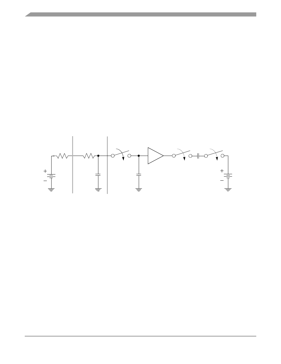
is a simplified model of an input channel. Refer to this model in the following discussion of
the interaction between the external circuitry and the circuitry inside the QADC.
Figure 28-53. Electrical Model of an A/D Input Signal
F
, R
SRC
, and C
F
comprise the external filter circuit. C
P
is the internal parasitic capacitor.
C
SAMP
is the capacitor array used to sample and hold the input voltage. V
I
is an internal voltage source
used to provide charge to C
SAMP
during sample phase.
The following paragraphs provide a simplified description of the interaction between the QADC and the
user's external circuitry. This circuitry is assumed to be a simple RC low-pass filter passing a signal from
a source to the QADC input signal. These paragraphs make the following assumptions:
•
The external capacitor is perfect (no leakage, no significant dielectric absorption characteristics,
etc.).
•
All parasitic capacitance associated with the input signal is included in the value of the external
capacitor.
•
Inductance is ignored.
•
The “on” resistance of the internal switches is 0 ohms and the “off” resistance is infinite.
S1
AMP
RF
S3
C
SAMP
V
I
C
P
C
F
V
SRC
Internal Circuit Model
External Filter
V
SRC
= Source Voltage
= Internal Parasitic Capacitance
RF
CF
CP
C
SAMP
= Sample Capacitor
VI
= Filter Impedance
= Filter Capacitor
= Internal Voltage Source During Sample and Hold
Source
R
SRC
R
SRC
= Source Impedance
S2
MCF5282 and MCF5216 ColdFire Microcontroller User’s Manual, Rev. 3