Motorola ColdFire MCF5281 User Manual
Page 244
Signal Descriptions
14-4
Freescale Semiconductor
SDRAM write enable
DRAMW
Asserted to signify that a DRAM write
cycle is underway. Negated to indicate
a read cycle.
O
SDRAM bank selects
SDRAM_CS[1:0]
Interface to the chip-select lines of the
SDRAMs within a memory block.
O
SDRAM clock enable
SCKE
SDRAM clock enable.
O
Clock and Reset Signals
Reset in
RSTI
Asserted to enter reset exception
processing.
I
Reset out
RSTO
Automatically asserted with RSTI.
Negation indicates that the PLL has
regained its lock.
O
EXTAL
EXTAL
Driven by an external clock except
when used as a connection to the
external crystal.
I
XTAL
XTAL
Internal oscillator connection to the
external crystal.
O
Clock output
CLKOUT
Reflects the system clock.
O
Chip Configuration Module
Clock mode
CLKMOD[1:0]
Clock mode select
I
Reset configuration
RCON
Reset configuration select
I
External Interrupt Signals
External interrupts
IRQ[7:1]
External interrupt sources.
I
Ethernet Module Signals
(not available on MCF5214 and MCF5216)
Management data
EMDIO
Transfers control information between
the external PHY and the media
access controller.
I/O
Management data clock EMDC
Provides a timing reference to the PHY
for data transfers on the EMDIO signal.
O
Transmit clock
ETXCLK
Provides a timing reference for
ETXEN, ETXD[3:0], and ETXER.
I
Transmit enable
ETXEN
Indicates when valid nibbles are
present on the MII.
O
Transmit data 0
ETXD0
Serial output Ethernet data.
O
Collision
ECOL
Asserted to indicate a collision.
I
Receive clock
ERXCLK
Provides a timing reference for
ERXDV, ERXD[3:0], and ERXER.
I
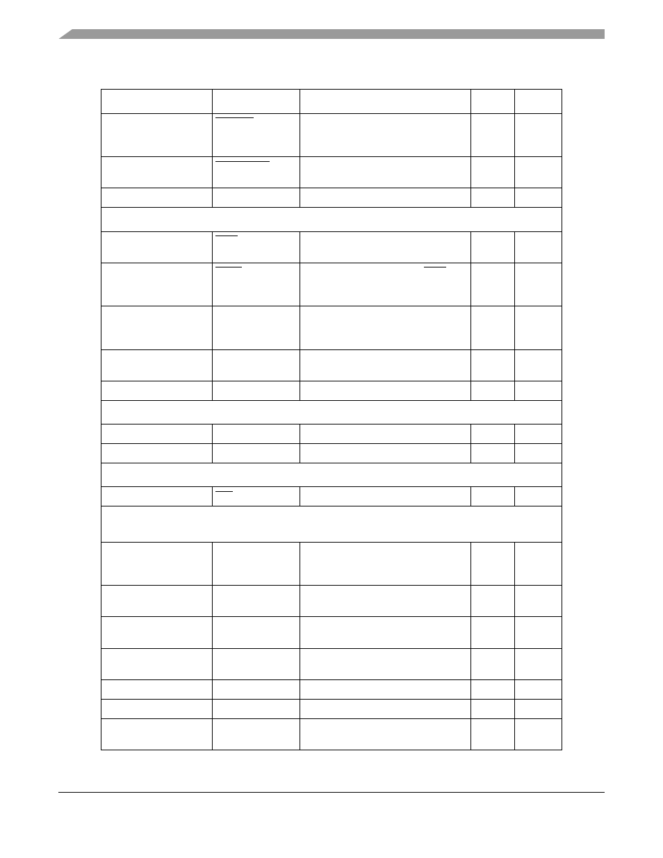
Table 14-1. MCF5282 Signal Description (continued)
Signal Name
Abbreviation
Function
I/O
Page
MCF5282 and MCF5216 ColdFire Microcontroller User’s Manual, Rev. 3