3 memory map/register definition, 1 qspi mode register (qmr), 3 memory map/register definition -3 – Motorola ColdFire MCF5281 User Manual
Page 407: 1 qspi mode register (qmr) -3
Queued Serial Peripheral Interface (QSPI)
Freescale Semiconductor
22-3
22.3
Memory Map/Register Definition
is the QSPI register memory map. Reading reserved locations returns zeros.
22.3.1
QSPI Mode Register (QMR)
The QMR, shown in
, determines the basic operating modes of the QSPI module. Parameters
such as QSPI_CLK polarity and phase, baud rate, master mode operation, and transfer size are determined
by this register.
NOTE
Because the QSPI does not operate in slave mode, the master mode enable
bit (QMR[MSTR]) must be set for the QSPI module to operate correctly.
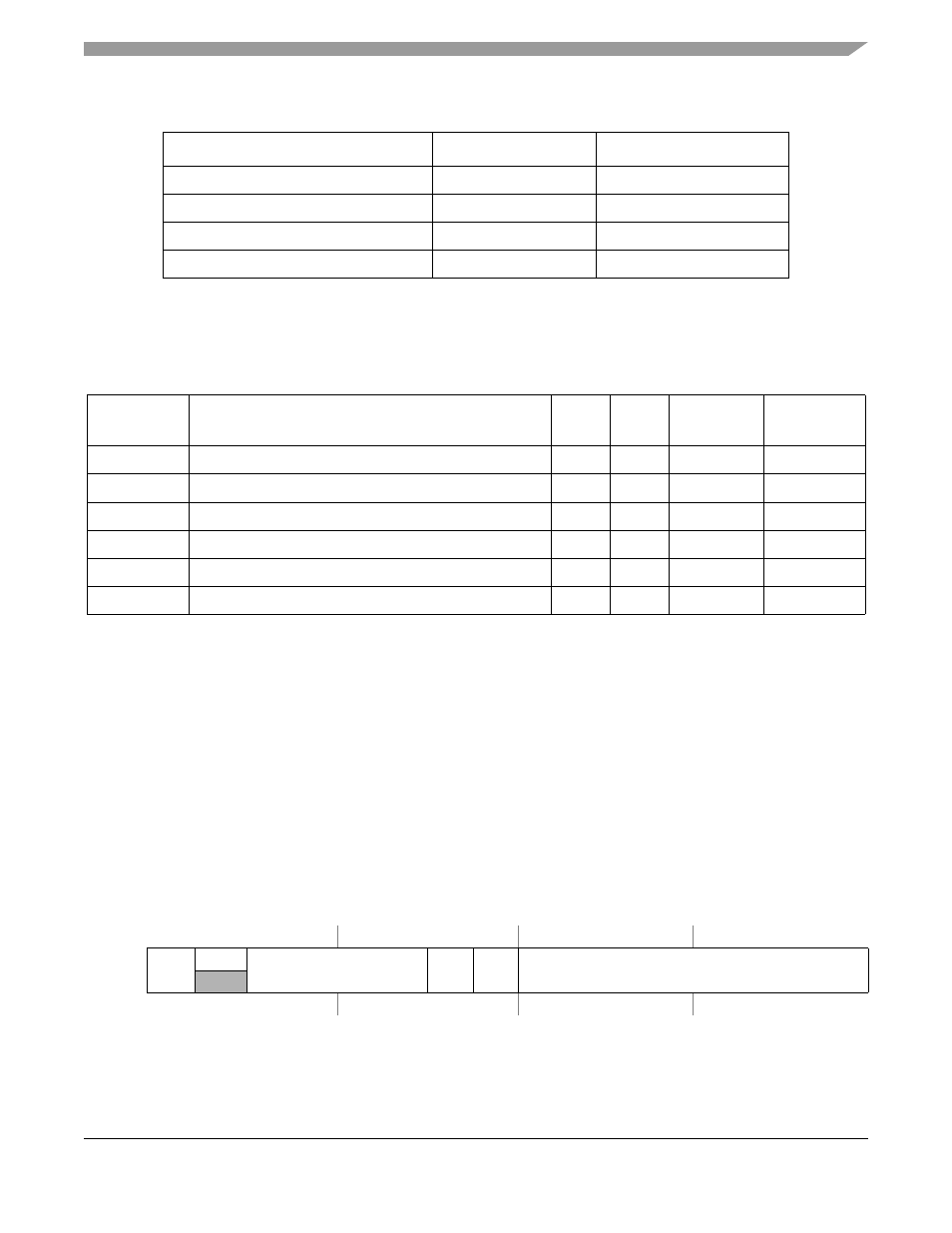
Table 22-1. QSPI Input and Output Signals and Functions
Signal Name
Hi-Z or Actively Driven
Function
Data output (QSPI_DOUT)
Configurable
Serial data output from QSPI
Data input (QSPI_DIN)
N/A
Serial data input to QSPI
Serial clock (QSPI_CLK)
Actively driven
Clock output from QSPI
Peripheral chip selects (QSPI_CSn)
Actively driven
Peripheral selects from QSPI
Table 22-2. QSPI Memory Map
IPSBAR
Offset
1
1
Addresses not assigned to a register and undefined register bits are reserved for expansion.
Register
Width
(bits)
Access
Reset Value
Section/Page
0x00_0340
QSPI Mode Register (QMR)
16
R/W
0x0104
0x00_0344
QSPI Delay Register (QDLYR)
16
R/W
0x0404
0x00_0348
QSPI Wrap Register (QWR)
16
R/W
2
2
See the register description for special cases. Some bits may be read- or write-only.
0x0000
0x00_034C
QSPI Interrupt Register (QIR)
16
R/W
0x0000
0x00_0350
QSPI Address Register (QAR)
16
R/W
0x0000
0x00_0354
QSPI Data Register (QDR)
16
R/W
0x0000
IPSBAR
Offset:
0x00_0340 (QMR)
Access: User read/write
15
14
13
12
11
10
9
8
7
6
5
4
3
2
1
0
R
MSTR
0
BITS
CPOL CPHA
BAUD
W
Reset
0
0
0
0
0
0
0
1
0
0
0
0
0
1
0
0
Figure 22-2. QSPI Mode Register (QMR)
MCF5282 and MCF5216 ColdFire Microcontroller User’s Manual, Rev. 3