1 data registers (d0-d7), 2 address registers (a0-a6), 1 data registers (d0–d7) – Motorola ColdFire MCF5281 User Manual
Page 50: 2 address registers (a0–a6)
ColdFire Core
2-4
Freescale Semiconductor
2.2.1
Data Registers (D0–D7)
D0–D7 data registers are for bit (1-bit), byte (8-bit), word (16-bit) and longword (32-bit) operations; they
can also be used as index registers.
NOTE
Registers D0 and D1 contain hardware configuration details after reset. See
Section 2.3.4.15, “Reset Exception”
for more details.
2.2.2
Address Registers (A0–A6)
These registers can be used as software stack pointers, index registers, or base address registers. They can
also be used for word and longword operations.
0x80F
Program Counter (PC)
32
R/W
Contents of
location
0x0000_0004
No
Supervisor Access Only Registers
0x002
Cache Control Register (CACR)
32
R/W
0x0000_0000
Yes
0x004–5
Access Control Register 0–1 (ACR0–1)
32
R/W
See Section
Yes
0x800
User/Supervisor A7 Stack Pointer
(OTHER_A7)
32
R/W
Contents of
location
0x0000_0000
No
0x801
Vector Base Register (VBR)
32
R/W
0x0000_0000
Yes
0x80E
Status Register (SR)
16
R/W
0x27--
No
0xC04
Flash Base Address Register
(FLASHBAR)
32
R/W
0x0000_0000
Yes
0xC05
RAM Base Address Register (RAMBAR)
32
R/W
See Section
Yes
1
The values listed in this column represent the Rc field used when accessing the core registers via the BDM port. For more
information see
.
BDM: Load: 0x080 + n; n = 0-7 (Dn)
Store: 0x180 + n; n = 0-7 (Dn)
Access: User read/write
BDM read/write
31 30 29 28 27 26 25 24 23 22 21 20 19 18 17 16 15 14 13 12 11 10
9
8
7
6
5
4
3
2
1
0
R
Data
W
Reset
(D2-D7)
– – – – – – – – – – – – – – – – – – – – – – – – – – – – – – – –
Reset
(D0, D1)
See
Section 2.3.4.15, “Reset Exception”
Figure 2-2. Data Registers (D0–D7)
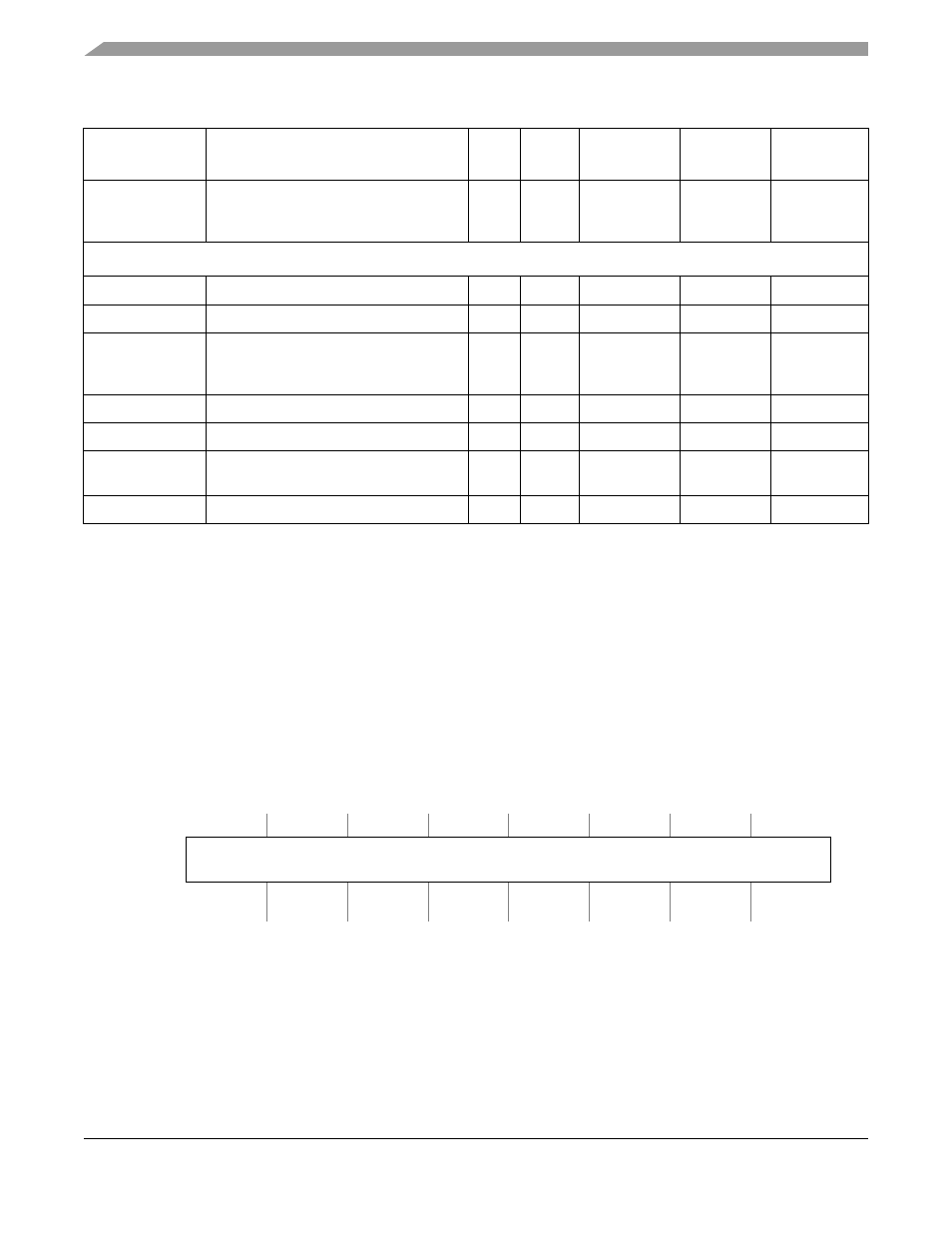
Table 2-1. ColdFire Core Programming Model (continued)
BDM
1
Register
Width
(bits)
Access
Reset Value
Written with
MOVEC
Section/Page
MCF5282 and MCF5216 ColdFire Microcontroller User’s Manual, Rev. 3