2 data transfer cycle states, 2 data transfer cycle states -4 – Motorola ColdFire MCF5281 User Manual
Page 228
External Interface Module (EIM)
13-4
Freescale Semiconductor
Basic operation of the bus is a three-clock bus cycle:
1. During the first clock, the address, attributes, and TS are driven.
2. Data and TA are sampled during the second clock of a bus-read cycle. During a read, the external
device provides data and is sampled at the rising edge at the end of the second bus clock. This data
is concurrent with TA, which is also sampled at the rising edge of the clock.
During a write, the ColdFire device drives data from the rising clock edge at the end of the first
clock to the rising clock edge at the end of the bus cycle. Wait states can be added between the first
and second clocks by delaying the assertion of TA. TA can be configured to be generated internally
through the CSCRs. If TA is not generated internally, the system must provide it externally.
3. The last clock of the bus cycle uses what would be an idle clock between cycles to provide hold
time for address, attributes and write data.
and
show the basic read and
write operations.
13.4.2
Data Transfer Cycle States
The data transfer operation is controlled by an on-chip state machine. Each bus clock cycle is divided into
two states. Even states occur when CLKOUT is high and odd states occur when CLKOUT is low. The state
transition diagram for basic and fast termination read and write cycles are shown in
.
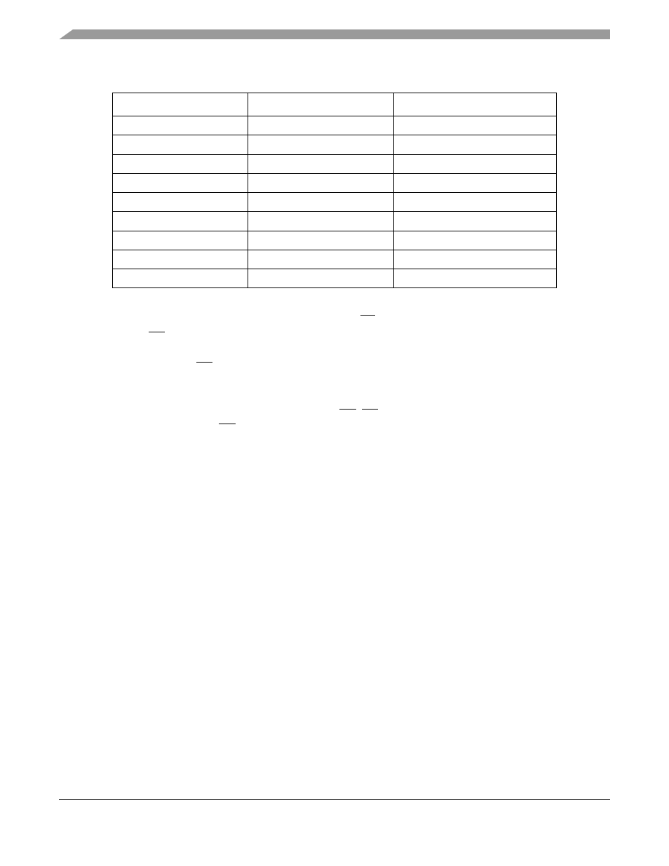
Table 13-2. Accesses by Matches in CSCRs and DACRs
Number of CSCR Matches
Number of DACR Matches
Type of Access
0
0
External
1
0
Defined by CSCR
Multiple
0
External, burst-inhibited, 32-bit
0
1
Defined by DACRs
1
1
Undefined
Multiple
1
Undefined
0
Multiple
Undefined
1
Multiple
Undefined
Multiple
Multiple
Undefined
MCF5282 and MCF5216 ColdFire Microcontroller User’s Manual, Rev. 3