2 dram address and control registers (dacr0/dacr1), P. 15-6 – Motorola ColdFire MCF5281 User Manual
Page 278
Synchronous DRAM Controller Module
15-6
Freescale Semiconductor
15.2.2.2
DRAM Address and Control Registers (DACR0/DACR1)
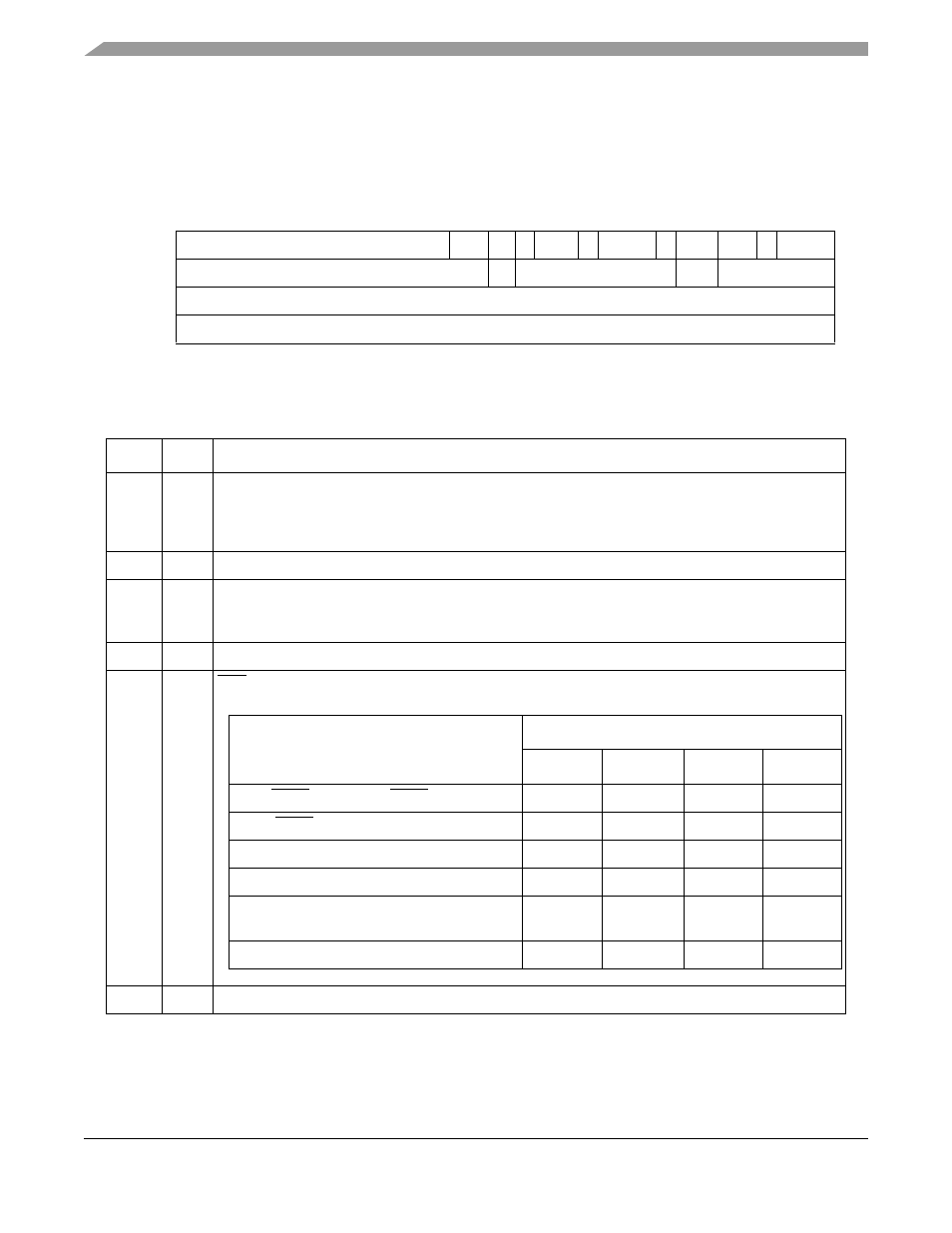
The DACRn registers, shown in
, contain the base address compare value and the control bits
for memory blocks 0 and 1 of the SDRAM controller. Address and timing are also controlled by bits in
DACRn.
describes DACRn fields.
31
18 17 16
15
14 13 12 11 10 9
8
7
6
5
4
3
2
0
Field
BA
—
RE — CASL —
CBM
— IMRS
PS
IP
—
Reset
Uninitialized
0
Uninitialized
0
Uninitialized
R/W
R/W
Address
IPSBAR+0x048 (DACR0); 0x050 (DACR1)
Figure 15-3. DRAM Address and Control Register (DACRn)
Table 15-5. DACRn Field Descriptions
Bit
Name
Description
31–18
BA
Base address register. With DCMR[BAM], determines the address range in which the associated
DRAM block is located. Each BA bit is compared with the corresponding address of the current bus
cycle. If all unmasked bits match, the address hits in the associated DRAM block. BA functions the
same as in asynchronous operation.
17–16
—
Reserved, should be cleared.
15
RE
Refresh enable. Determines when the DRAM controller generates a refresh cycle to the DRAM block.
0 Do not refresh associated DRAM block
1 Refresh associated DRAM block
14
—
Reserved, should be cleared.
13–12
CASL CAS latency. Affects the following SDRAM timing specifications. Timing nomenclature varies with
manufacturers. Refer to the SDRAM specification for the appropriate timing nomenclature:
Parameter
Number of Bus Clocks
CASL= 00 CASL = 01 CASL= 10
CASL= 11
t
RCD
—SRAS assertion to SCAS assertion
1
2
3
3
t
CASL
—SCAS assertion to data out
1
2
3
3
t
RAS
—
ACTV
command to precharge command
2
4
6
6
t
RP
—Precharge command to
ACTV
command
1
2
3
3
t
RWL
,
t
RDL
—Last data input to precharge
command
1
1
1
1
t
EP
—Last data out to precharge command
1
1
1
1
11
—
Reserved, should be cleared.
MCF5282 and MCF5216 ColdFire Microcontroller User’s Manual, Rev. 3