11 reset and configuration override timing, 11reset and configuration override timing -19 – Motorola ColdFire MCF5281 User Manual
Page 703

Electrical Characteristics
Freescale Semiconductor
33-19
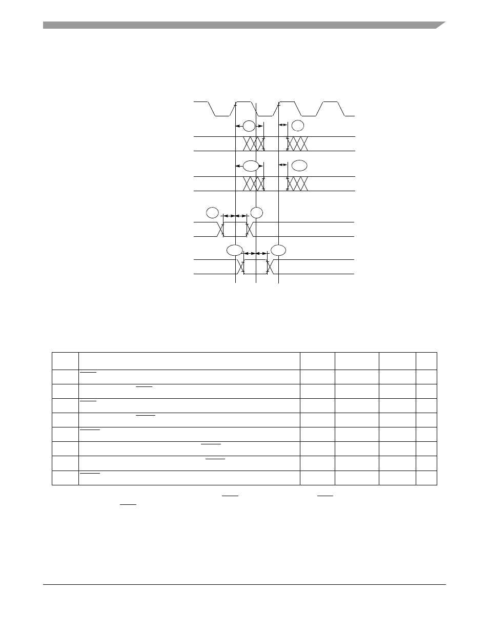
Figure 33-8. GPIO Timing
33.11 Reset and Configuration Override Timing
1
GPIO pins include: Ports A-I, INT, SPI, SCI1/2 (including SCI functions), FlexCAN and Timer.
2
Because of long delays associated with the PQA/PQB pads, signals on the PQA/PQB pins will be updated on the
following edge of the clock.
Table 33-18. Reset and Configuration Override Timing
(V
DD
= 2.7 to 3.6 V, V
SS
= 0 V)
1
1
All AC timing is shown with respect to 50% V
DD
levels unless otherwise noted.
NUM
Characteristic
Symbol
Min
Max
Unit
R1
RSTI Input valid to CLKOUT High
t
RVCH
10
—
ns
R2
CLKOUT High to RSTI Input invalid
t
CHRI
2
—
ns
R3
RSTI Input valid Time
2
2
During low-power STOP, the synchronizers for the RSTI input are bypassed and RSTI is asserted asynchronously to
the system. Thus, RSTI must be held a minimum of 100 ns.
t
RIVT
5
—
t
CYC
R4
CLKOUT High to RSTO Valid
t
CHROV
—
12
ns
R5
RSTO valid to Config. Overrides valid
t
ROVCV
0
—
ns
R6
Configuration Override Setup Time to RSTO invalid
t
COS
20
—
t
CYC
R7
Configuration Override Hold Time after RSTO invalid
t
COH
0
—
ns
R8
RSTO invalid to Configuration Override High Impedance
t
ROICZ
—
1
t
CYC
G1
CLKOUT
GPIO Outputs
G2
PQA/PQB Outputs
G2a
G3a
G4a
PQA/PQB Inputs
G3
G4
GPIO Inputs
G1a
MCF5282 and MCF5216 ColdFire Microcontroller User’s Manual, Rev. 3
