3 read cycle, 3 read cycle -6 – Motorola ColdFire MCF5281 User Manual
Page 230
External Interface Module (EIM)
13-6
Freescale Semiconductor
NOTE
An external device has at most two CLKOUT cycles after the start of S4 to
three-state the data bus. This applies to basic read cycles, fast termination
cycles, and the last transfer of a burst.
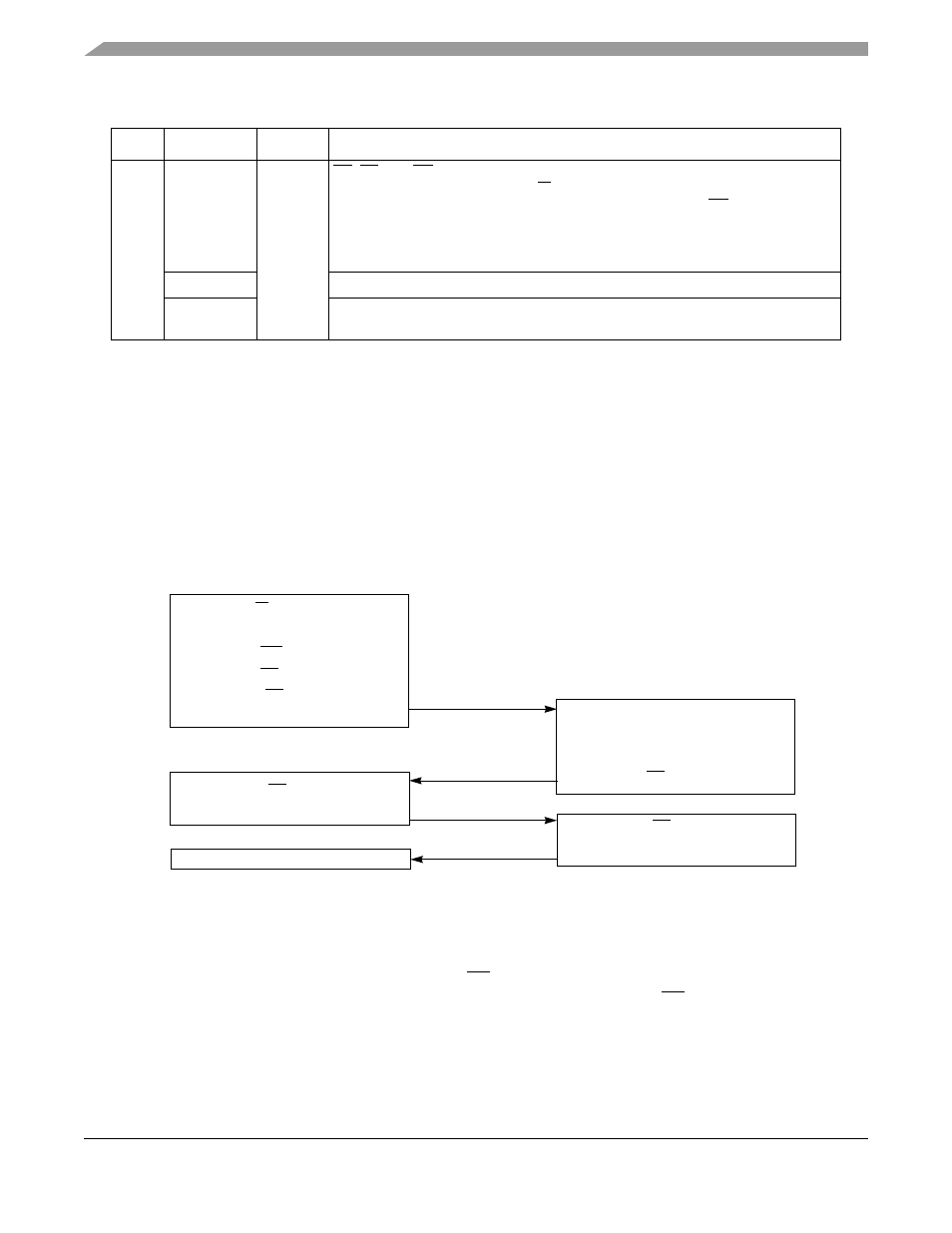
13.4.3
Read Cycle
During a read cycle, the device receives data from memory or from a peripheral device.
is a
read cycle flowchart.
Figure 13-5. Read Cycle Flowchart
The read cycle timing diagram is shown in
NOTE
In the following timing diagrams, TA waveforms apply for chip selects
programmed to enable either internal or external termination. TA assertion
should look the same in either case.
S5
S5
Low
CS, BS, and OE are negated on the CLKOUT falling edge of S5. The processor
stops driving address lines and R/W on the rising edge of CLKOUT, terminating the
read or write cycle. At the same time, the processor negates TIP, and SIZ[1:0] on
the rising edge of CLKOUT.
Note that the rising edge of CLKOUT may be the start of S0 for the next access
cycle.
Read
The external device stops driving data between S4 and S5.
Write
The data bus returns to high impedance on the rising edge of CLKOUT. The rising
edge of CLKOUT may be the start of S0 for the next access.
Table 13-3. Bus Cycle States (continued)
State
Cycle
CLKOUT
Description
External device
1.
Set R/W to read
2.
Place address on A[31:0]
3.
Assert TIP, and SIZ[1:0]
4.
Assert TS
5.
Negate TS
1.
Decode address and select the
appropriate slave device.
2.
Drive data on D[31:0]
3.
Assert TA
1.
Sample TA low and latch data
1.
Negate TA.
2.
Stop driving D[31:0]
1.
Start next cycle
ColdFire processor
MCF5282 and MCF5216 ColdFire Microcontroller User’s Manual, Rev. 3