5 auto-refresh operation, 5 auto-refresh operation -15, Figure 15-7 – Motorola ColdFire MCF5281 User Manual
Page 287: Shows the burst write
Synchronous DRAM Controller Module
Freescale Semiconductor
15-15
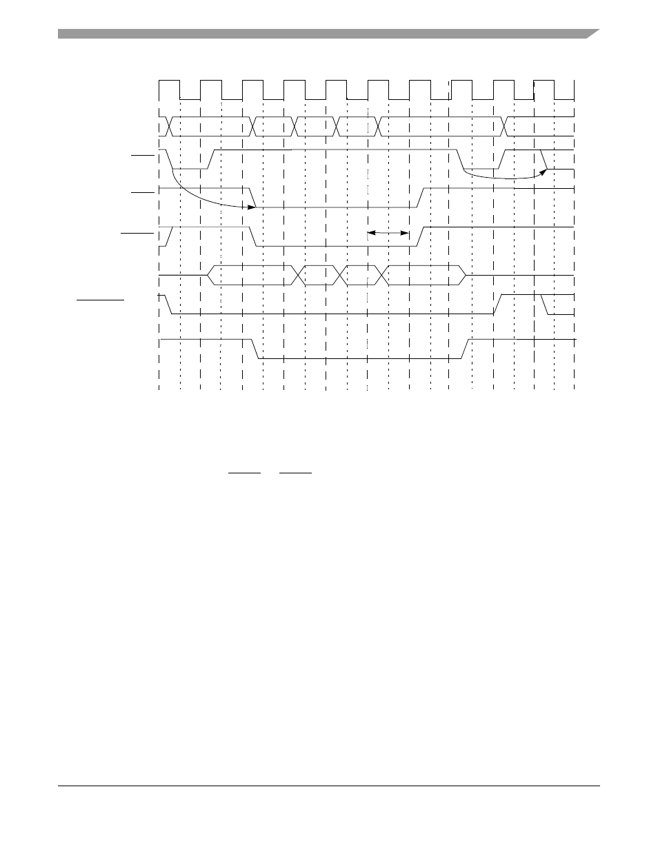
Figure 15-7. Burst Write SDRAM Access
Accesses in synchronous burst page mode always cause the following sequence:
1.
ACTV
command
2.
NOP
commands to assure SRAS-to-SCAS delay (if CAS latency is 1, there are no
NOP
commands).
3. Required number of
READ
or
WRITE
commands to service the transfer size with the given port
size.
4. Some transfers need more
NOP
commands to assure the
ACTV
-to-precharge delay.
5.
PALL
command
6. Required number of idle clocks inserted to assure precharge-to-
ACTV
delay.
15.2.3.5
Auto-Refresh Operation
The DRAM controller is equipped with a refresh counter and control. This logic is responsible for
providing timing and control to refresh the SDRAM without user interaction. Once the refresh counter is
set, and refresh is enabled, the counter counts to zero. At this time, an internal refresh request flag is set
and the counter begins counting down again. The DRAM controller completes any active burst operation
and then performs a
PALL
operation. The DRAM controller then initiates a refresh cycle and clears the
refresh request flag. This refresh cycle includes a delay from any precharge to the auto-refresh command,
the auto-refresh command, and then a delay until any
ACTV
command is allowed. Any SDRAM access
initiated during the auto-refresh cycle is delayed until the cycle is completed.
A[23:0]
SRAS
SCAS
DRAMW
D[31:0]
ACTV
WRITE
PALL
NOP
SDRAM_CS[0] or [1]
BS[3:0]
t
CASL
= 2
Row
Column
Column Column
Column
t
RP
t
RWL
CLKOUT
NOP
WRITE
WRITE
WRITE
MCF5282 and MCF5216 ColdFire Microcontroller User’s Manual, Rev. 3