4 write cycle, 4 write cycle -7, Figure 13-6 – Motorola ColdFire MCF5281 User Manual
Page 231: N in
External Interface Module (EIM)
Freescale Semiconductor
13-7
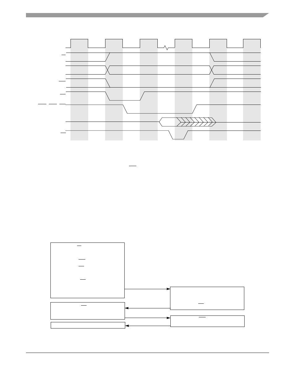
Figure 13-6. Basic Read Bus Cycle
Note the following characteristics of a basic read:
•
In S3, data is made available by the external device on the falling edge of CLKOUT and is sampled
on the rising edge of CLKOUT with TA asserted.
•
In S4, the external device can stop driving data after the rising edge of CLKOUT. However data
could be driven up to S5.
•
For a read cycle, the external device stops driving data between S4 and S5.
.
13.4.4
Write Cycle
During a write cycle, the processor sends data to the memory or to a peripheral device. The write cycle
flowchart is shown in
.
Figure 13-7. Write Cycle Flowchart
R/W
TIP
TS
D[31:0]
TA
Read
S0
S1
S2
S3
S4
S5
CLKOUT
CSn, BSn, OE
A[31:0], SIZ[1:0]
External Device
1.
Set R/W to write
2.
Place address on A[31:0]
3.
Assert TIP and SIZ[1:0]
4.
Assert TS
5.
Place data on D[31:0]
6.
Negate TS
1.
Decode address
2.
Store data on D[31:0]
3.
Assert TA
1.
Sample TA low
2.
Stop driving data from D[31:0]
1.
Negate TA
1.
Start next cycle
ColdFire processor
MCF5282 and MCF5216 ColdFire Microcontroller User’s Manual, Rev. 3