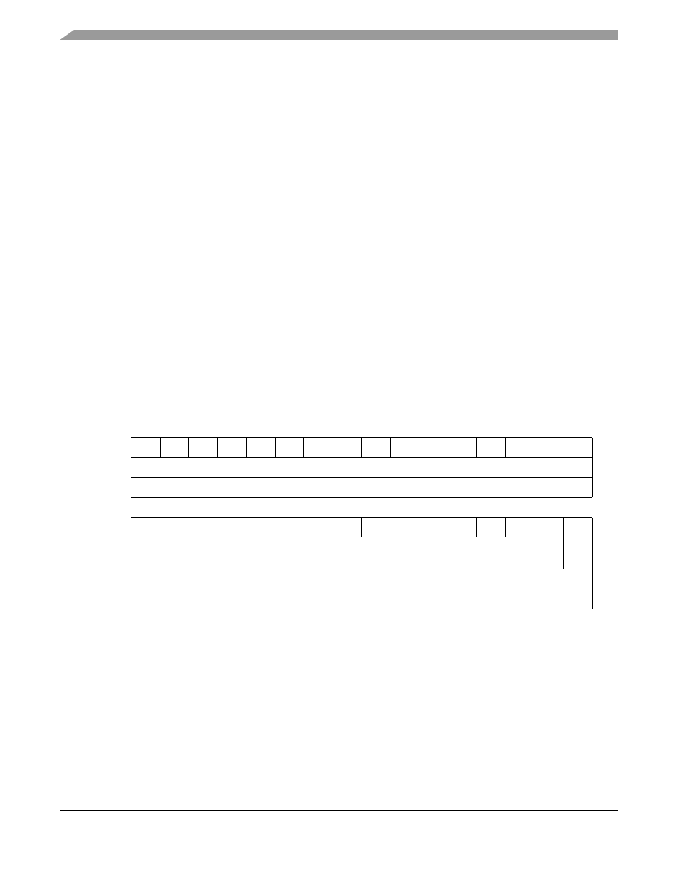
Figure 6-3 – Motorola ColdFire MCF5281 User Manual
Page 118

ColdFire Flash Module (CFM)
6-6
Freescale Semiconductor
NOTE
Flash accesses (reads/writes) by a bus master other than the core, (DMA
controller or Fast Ethernet Controller), or writes to Flash by the core during
programming must use the backdoor Flash address of IPSBAR plus an
offset of 0x0400_0000. For example, for a DMA transfer from the first
location of Flash when IPSBAR is still at its default location of
0x4000_0000, the source register would be loaded with 0x4400_0000.
Backdoor access to Flash for reads can be made by the bus master, but it
takes 2 cycles longer than a direct read of the Flash if using its FLASHBAR
address.
NOTE
The Flash is marked as valid on reset based on the RCON (reset
configuration) pin state. Flash space is valid on reset when booting in single
chip mode (RCON pin asserted and D[26]/D[17]/D[16] set to 110), or when
booting internally in master mode (RCON asserted and D[26]/D[17]/D[16]
are set to 111 and D[18] and D[19] are set to 00). See
” for more details. When the default reset
configuration is not overriden, the device (by default) boots in single chip
mode and the Flash space will be marked as valid at address 0x0. The Flash
configuration field is checked during the reset sequence to see if the Flash
is secured. If it is the part will always boot from internal Flash, since it will
be marked as valid, regardless of what is done for chip configuration.
31
30
29
28
27
26
25
24
23
22
21
20
19
18
16
Field BA31 BA30 BA29 BA28 BA27 BA26 BA25 BA24 BA23 BA22 BA21 BA20 BA19
—
Reset
0000_0000_0000_0000
R/W
R/W
15
9
8
7
6
5
4
3
2
1
0
Field
—
WP
—
C/I
SC
SD
UC
UD
V
Reset
0000_0001_0010_000
See
Note
R/W
R
R/W
Address
CPU + 0xC04
Note: The reset value for the valid bit is determined by the chip mode selected at reset (see
“Chip Configuration Module (CCM)
”).
Figure 6-3. Flash Base Address Register (FLASHBAR)
MCF5282 and MCF5216 ColdFire Microcontroller User’s Manual, Rev. 3
