Motorola ColdFire MCF5281 User Manual
Page 735

Register Memory Map
Freescale Semiconductor
A-23
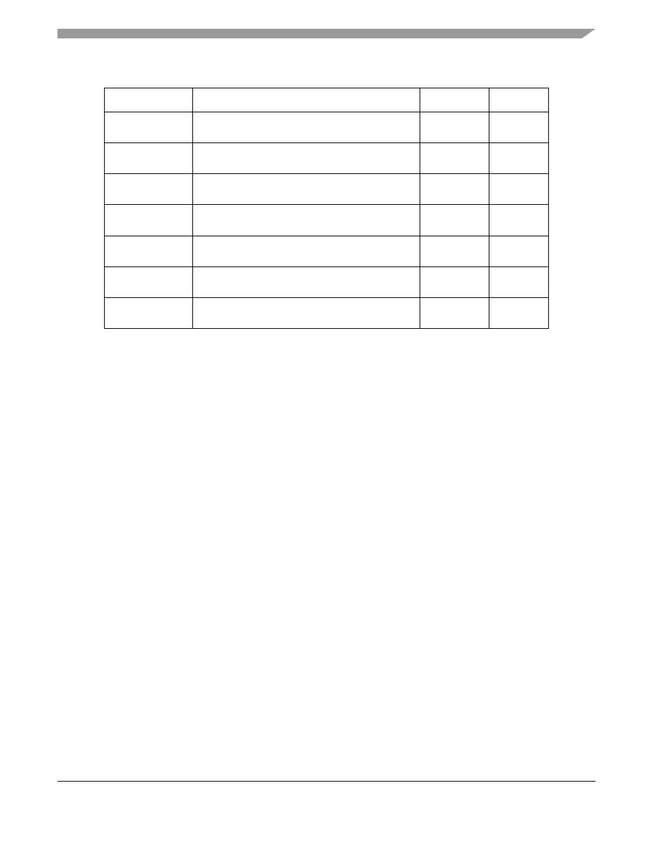
IPSBAR +
0x1D_0002
CFM Clock Divider Register
CFMCLKD
8
IPSBAR +
0x1D_0008
CFM Security Register
CFMSEC
32
IPSBAR +
0x1D_0010
CFM Protection Register
CFMPROT
32
IPSBAR +
0x1D_0014
CFM Supervisor Access Register
CFMSACC
32
IPSBAR +
0x1D_0018
CFM Data Access Register
CFMDACC
32
IPSBAR +
0x1D_0020
CFM User Status Register
CFMUSTAT
8
IPSBAR +
0x1D_0024
CFM Command Register
CFMCMD
8
1
The DMA module originally supported a left-justified 16-bit byte count register (BCR). This function was
later reimplemented as a right-justified 24-bit BCR. The operation of the DMA and the interpretation of
the BCR is controlled by the MPARK[BCR24BIT]. See
Chapter 8, “System Control Module (SCM)
” for
more details.
2
UMR1n, UMR2n, and UCSRn should be changed only after the receiver/transmitter is issued a software
reset command. That is, if channel operation is not disabled, undesirable results may occur.
Table A-3. Register Memory Map (continued)
Address
Name
Mnemonic
Size
MCF5282 and MCF5216 ColdFire Microcontroller User’s Manual, Rev. 3
