Motorola ColdFire MCF5281 User Manual
Page 274
Synchronous DRAM Controller Module
15-2
Freescale Semiconductor
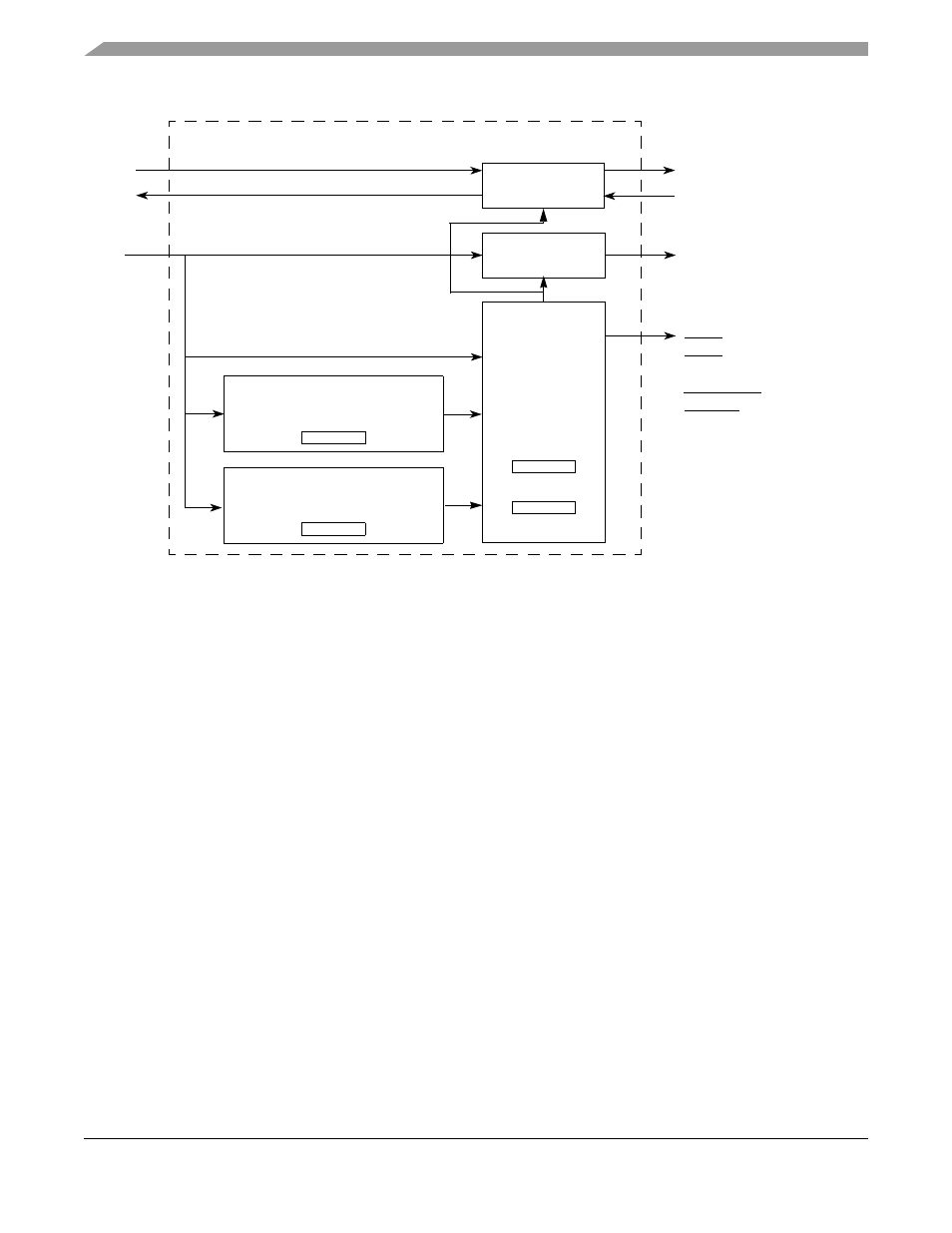
Figure 15-1. Synchronous DRAM Controller Block Diagram
The DRAM controller’s major components are as follows:
•
DRAM address and control registers (DACR0 and DACR1)—The DRAM controller consists of
two configuration register units, one for each supported memory block. DACR0 is accessed at
IPSBAR + 0x048; DACR1 is accessed at IPSBAR + 0x050. The register information is passed on
to the hit logic.
•
Control logic and state machine—Generates all SDRAM signals, taking hit information and
bus-cycle characteristic data from the block logic in order to generate SDRAM accesses. Handles
refresh requests from the refresh counter.
— DRAM control register (DCR)—Contains data to control refresh operation of the DRAM
controller. Both memory blocks are refreshed concurrently as controlled by DCR[RC].
— Refresh counter—Determines when refresh should occur; controlled by the value of DCR[RC].
It generates a refresh request to the control block.
•
Hit logic—Compares address and attribute signals of a current SDRAM bus cycle to both DACRs
to determine if an SDRAM block is being accessed. Hits are passed to the control logic along with
characteristics of the bus cycle to be generated.
•
Address multiplexing—Multiplexes addresses to allow column and row addresses to share pins.
This allows glueless interface to SDRAMs.
•
Data Generation—Controls the data input and data output transmission between the on-platform
and off-platform data buses.
Memory Block 0 Hit Logic
DRAM Address/Control Register 0
(DACR0)
A[23:0]
Internal
Address
Control Logic
and
DRAMW
DRAM Controller Module
Refresh Counter
SCAS
SRAS
SCKE
State Machine
Multiplexing
DRAM Control
Register (DCR)
Bus
Memory Block 1 Hit Logic
DRAM Address/Control Register 1
(DACR1)
A[23:0]
SDRAM_CS[1:0]
BS[3:0]
Data
Generation
D[31:0] internal
Q[31:0] internal
D[31:0]
D[31:0]
MCF5282 and MCF5216 ColdFire Microcontroller User’s Manual, Rev. 3