3 block diagram, 4 signal descriptions, 1 rcon – Motorola ColdFire MCF5281 User Manual
Page 530: 2 clkmod[1:0, 3 block diagram -2 27.4 signal descriptions -2, 2 clkmod[1:0] -2
Chip Configuration Module (CCM)
27-2
Freescale Semiconductor
27.3
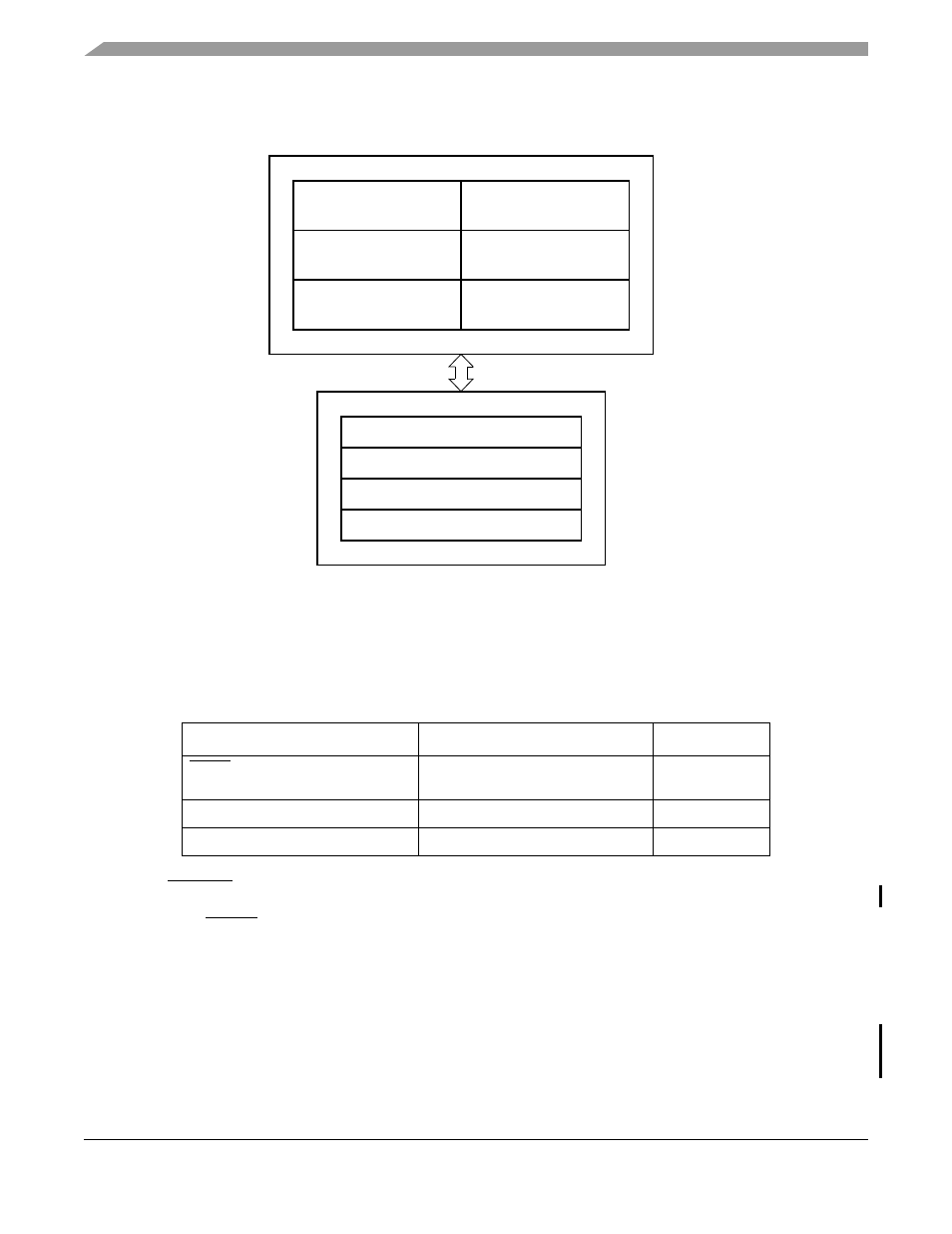
Block Diagram
Figure 27-1. Chip Configuration Module Block Diagram
27.4
Signal Descriptions
provides an overview of the CCM signals.
27.4.1
RCON
If the external RCON pin is asserted during reset, then various chip functions, including the reset
configuration pin functions after reset, are configured according to the levels driven onto the external data
pins. (see
Section 27.6, “Functional Description
”). The internal configuration signals are driven to reflect
the levels on the external configuration pins to allow for module configuration.
27.4.2
CLKMOD[1:0]
The state of the CLKMOD[1:0] pins during reset determines the clock mode.
Table 27-1. Signal Properties
Name
Function
Reset State
RCON
Reset configuration select
Internal weak
pull-up device
CLKMOD[1:0]
Clock mode select
—
D[26:24, 21, 19:16]
Reset configuration override pins
—
Reset
Chip Mode
Selection
Boot Device / Port
Size Selection
Output Pad
Strength Selection
Clock Mode
Selection
Chip Select
Configuration
Configuration
Reset Configuration Register
Chip Configuration Register
Chip Identification Register
Chip Test Register
MCF5282 and MCF5216 ColdFire Microcontroller User’s Manual, Rev. 3