2 external boot chip select operation, 4 chip select registers, 2 external boot chip select operation -4 – Motorola ColdFire MCF5281 User Manual
Page 218: 4 chip select registers -4, Figure 12-1
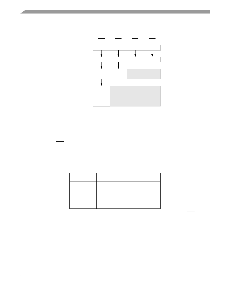
Chip Select Module
12-4
Freescale Semiconductor
between the data bus and the external byte strobe control lines (BS[3:0]). Note that all byte lanes are
driven, although the state of unused byte lanes is undefined.
Figure 12-1. Connections for External Memory Port Sizes
12.3.1.2
External Boot Chip Select Operation
CS0, the external boot chip select, allows address decoding for boot ROM before system initialization. Its
operation differs from other external chip select outputs after system reset.
After system reset, CS0 is asserted for every external access. No other chip select can be used until the
valid bit, CSMR0[V], is set, at which point CS0 functions as configured and CS[6:1] can be used. At reset,
the port size function of the external boot chip select is determined by the logic levels of the inputs on
D[19:18].
and
list the various reset encodings for the configuration signals
multiplexed with D[19:18].
Provided the required address range is in the chip select address register (CSAR0), CS0 can be
programmed to continue decoding for a range of addresses after the CSMR0[V] is set, after which the
external boot chip select can be restored only by a system reset.
12.4
Chip Select Registers
shows the chip select register memory map. Reading reserved locations returns zeros.
Table 12-4. D[19:18] External Boot Chip Select Configuration
D[19:18]
Boot Device/Data Port Size
00
Internal (32-bit)
01
External (16-bit)
10
External (8-bit)
11
External (32-bit)
Byte 0
8-bit port
16-bit port
32-bit port
Byte 1
Byte 2
Byte 3
Byte 0
Byte 1
Byte 2
Byte 3
Byte 0
Byte 1
Byte 2
Byte 3
D[31:24]
D[23:16]
D[15:8]
D[7:0]
External
memory
memory
memory
data bus
BS3
BS2
BS1
BS0
Driven, undefined
Driven, undefined
MCF5282 and MCF5216 ColdFire Microcontroller User’s Manual, Rev. 3