2 port data direction registers (ddrn), 2 port data direction registers (ddrn) -11, Figure 26-6 – Motorola ColdFire MCF5281 User Manual
Page 511: 2 port data direction registers (ddr n ), Port n bits are described in table 26-3
General Purpose I/O Module
Freescale Semiconductor
26-11
PORTn bits are described in
26.3.2.2
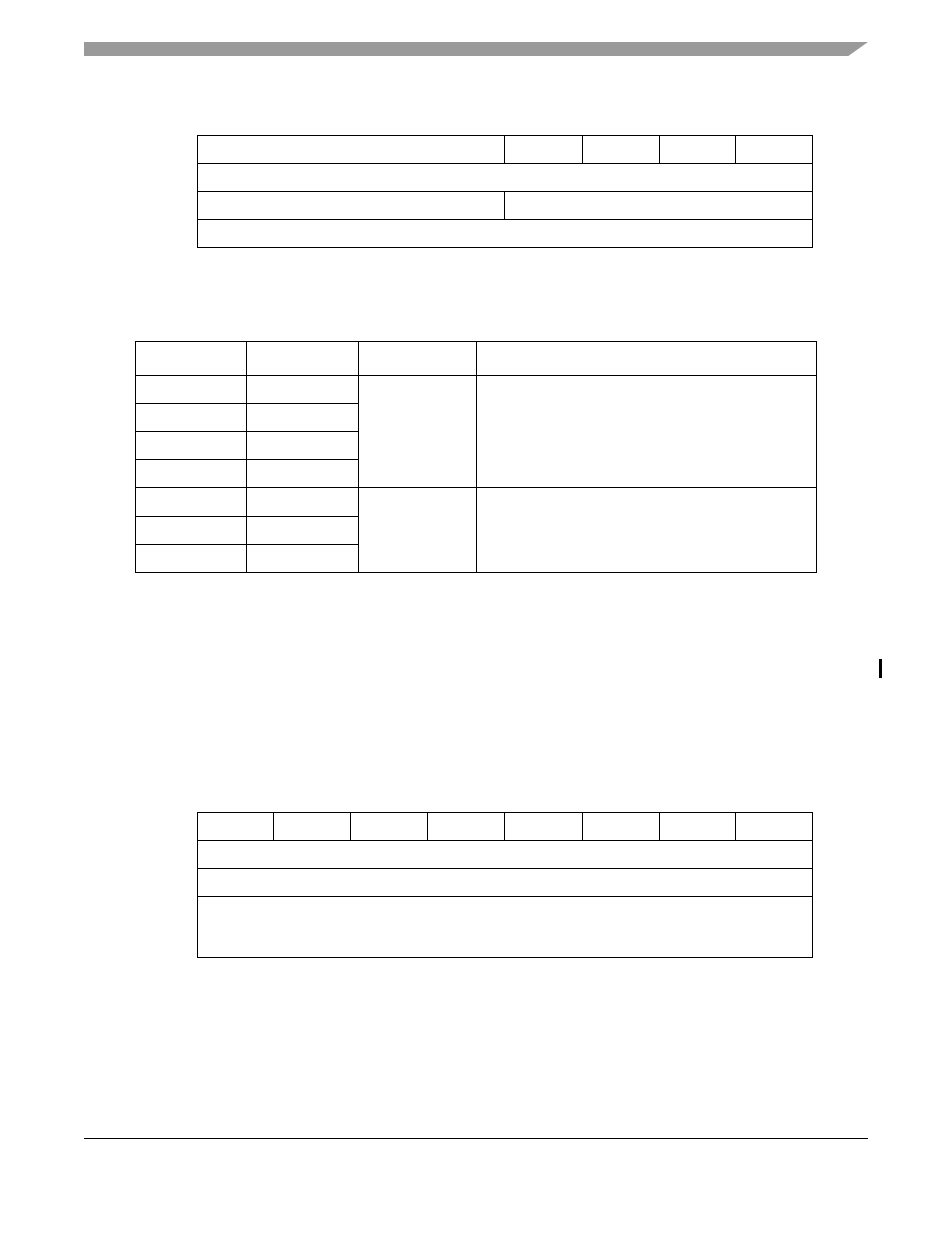
Port Data Direction Registers (DDRn)
The DDRs control the direction of the port n pin drivers when the pins are configured for digital I/O.
Most DDRs have a full 8-bit implementation, as shown in
. The remaining DDRs use fewer
than eight bits. Their bit definitions are shown in
The DDRs are read/write. At reset, all bits in the DDRs are cleared.
Setting any bit in a DDRn register configures the corresponding port n pin as an output. Clearing any bit
in a DDRn register configures the corresponding pin as an input.
7
4
3
2
1
0
Field
—
PORTn3
PORTn2
PORTn1
PORTn0
Reset
0000_1111
R/W:
R
R/W
Address
IPSBAR + 0x10_000F (PORTTC), 0x10_0010 (PORTTD), 0x10_0011 (PORTUA)
Figure 26-6. Port Output Data Registers (4-bit)
Table 26-3. PORTn (8-bit, 7-bit, 6-bit, and 4-bit) Field Descriptions
Register
Bits
Name
Description
8-bit
7–0
PORTnx
Port output data bits.
1 Drives 1 when the port n pin is a digital output
0 Drives 0 when the port n pin is a digital output
7-bit
6–0
6-bit
5–0
4-bit
3–0
7-bit
7
—
Reserved, should be cleared.
6-bit
7–6
4-bit
7–4
7
6
5
4
3
2
1
0
Field
DDRn7
DDRn6
DDRn5
DDRn4
DDRn3
DDRn2
DDRn1
DDRn0
Reset
0000_0000
R/W:
R/W
Address
IPSBAR + 0x10_0014 (DDRA), 0x10_0015 (DDRB), 0x10_0016 (DDRC), 0x10_0017 (DDRD),
0x10_0018 (DDRE), 0x10_0019 (DDRF), 0x10_001A (DDRG), 0x10_001B (DDRH),
0x10_001C (DDRJ), 0x10_001D (DDRDD), 0x10_001E (DDREH), 0x10_001F (DDREL)
Figure 26-7. Port Data Direction Registers (8-bit)
MCF5282 and MCF5216 ColdFire Microcontroller User’s Manual, Rev. 3