Motorola ColdFire MCF5281 User Manual
Page 110
Static RAM (SRAM)
5-2
Freescale Semiconductor
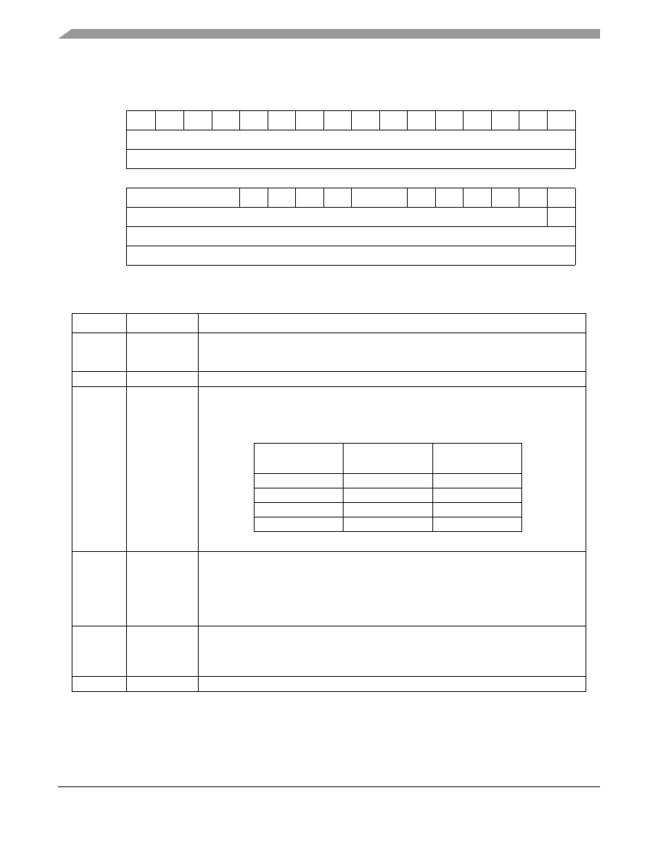
The RAMBAR contains several control fields. These fields are shown in
31
30
29
28
27
26
25
24
23
22
21
20
19
18
17
16
Field BA31 BA30 BA29 BA28 BA27 BA26 BA25 BA24 BA23 BA22 BA21 BA20 BA19 BA18 BA17 BA16
Reset
Undefined
R/W
W
15
14
13
12
11
10
9
8
7
6
5
4
3
2
1
0
Field
—
PRI1 PRI2 SPV
WP
—
C/I
SC
SD
UC
UD
V
Reset
Undefined
0
R/W
W
Address
CPU + 0xC05
Figure 5-1. SRAM Base Address Register (RAMBAR)
Table 5-1. SRAM Base Address Register
Bits
Name
Description
31–16
BA
Base address. Defines the 0-modulo-64K base address of the SRAM module. By
programming this field, the SRAM may be located on any 64-Kbyte boundary within the
processor’s 4-Gbyte address space.
15–12
—
Reserved, should be cleared.
11–10
PRI1, PRI2
Priority bit. PRI1 determines if DMA or CPU has priority in upper 32k bank of memory. PRI2
determines if DMA or CPU has priority in lower 32k bank of memory. If bit is set, CPU has
priority. If bit is cleared, DMA has priority. Priority is determined according to the following
table.
NOTE: The Freescale-recommended setting for the priority bits is 00.
9
SPV
Secondary port valid. Allows access by DMA
0 DMA access to memory is disabled.
1 DMA access to memory is enabled.
NOTE: The BDE bit in the second RAMBAR register must also be set to allow dual port
access to the SRAM. For more information, see
Section 8.4.2, “Memory Base Address
.”
8
WP
Write protect. Allows only read accesses to the SRAM. When this bit is set, any attempted
write access will generate an access error exception to the ColdFire processor core.
0 Allows read and write accesses to the SRAM module
1 Allows only read accesses to the SRAM module
7–6
—
Reserved, should be cleared.
PRI[1:2]
Upper Bank
Priority
Lower Bank
Priority
00
DMA Accesses
DMA Accesses
01
DMA Accesses
CPU Accesses
10
CPU Accesses
DMA Accesses
11
CPU Accesses
CPU Accesses
MCF5282 and MCF5216 ColdFire Microcontroller User’s Manual, Rev. 3