Motorola ColdFire MCF5281 User Manual
Page 373
General Purpose Timer Modules (GPTA and GPTB)
Freescale Semiconductor
20-5
20.5.1
GPT Input Capture/Output Compare Select Register (GPTIOS)
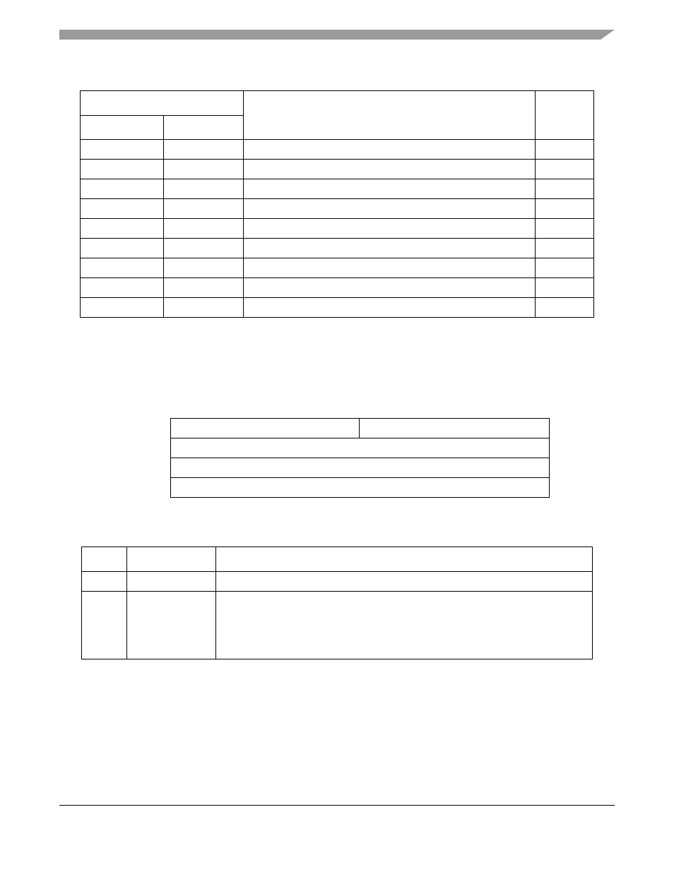
0x1A_0017
0x1B_0017
GPT Channel 3 Register Low (GPTC3L)
S
0x1A_0018
0x1B_0018
Pulse Accumulator Control Register (GPTPACTL)
S
0x1A_0019
0x1B_0019
Pulse Accumulator Flag Register (GPTPAFLG)
S
0x1A_001A
0x1B_001A
Pulse Accumulator Counter Register High (GPTPACNTH)
S
0x1A_001B
0x1B_001B
Pulse Accumulator Counter Register Low (GPTPACNTL)
S
0x1A_001C
0x1B_001C
Reserved
(2)
—
0x1A_001D
0x1B_001D
GPT Port Data Register (GPTPORT)
S
0x1A_001E
0x1B_001E
GPT Port Data Direction Register (GPTDDR)
S
0x1A_001F
0x1B_001F
GPT Test Register (GPTTST)
S
1
S = CPU supervisor mode access only.
2
Writes have no effect, reads return 0s, and the access terminates without a transfer error exception.
7
4
3
0
Field
—
IOS
Reset
0000_0000
R/W
R/W
Address
IPSBAR + 0x401A_0000, 0x401B_0000
Figure 20-2. GPT Input Capture/Output Compare Select Register (GPTIOS)
Table 20-4. GPTIOS Field Descriptions
Bit(s)
Name
Description
7–4
—
Reserved, should be cleared.
3–0
IOS
I/O select. The IOS[3:0] bits enable input capture or output compare operation for the
corresponding timer channels. These bits are read anytime (always read 0x00), write
anytime.
1 Output compare enabled
0 Input capture enabled
Table 20-3. GPT Modules Memory Map (continued)
IPSBAR Offset
Bits 7–0
Access
1
GPTA
GPTB
MCF5282 and MCF5216 ColdFire Microcontroller User’s Manual, Rev. 3