Of 2 system clock cycles. because t, S are executed until the last data is read. a, Delay completes – Motorola ColdFire MCF5281 User Manual
Page 286
Synchronous DRAM Controller Module
15-14
Freescale Semiconductor
Note that in synchronous operation, burst mode and address incrementing during burst cycles are
controlled by the DRAM controller. Thus, instead of the SDRAM enabling its internal burst incrementing
capability, the processor controls this function. This means that the burst function that is enabled in the
mode register of SDRAMs must be disabled when interfacing to the processor.
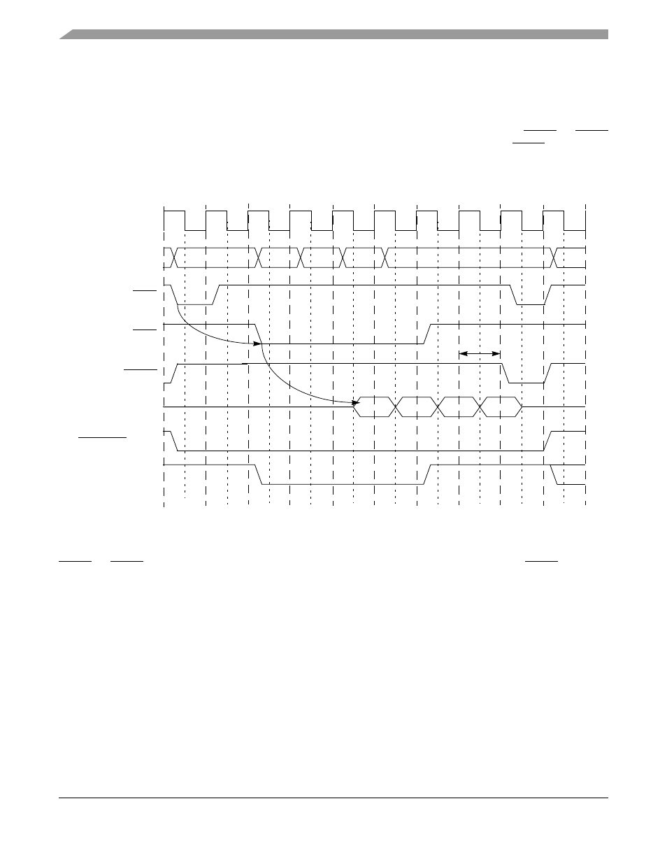
shows a burst read operation. In this example, DACR[CASL] = 01 for an SRAS-to-SCAS
delay (t
RCD
) of 2 system clock cycles. Because t
RCD
is equal to the read CAS latency (SCAS assertion to
data out), this value is also 2 system clock cycles. Notice that
NOP
s are executed until the last data is read.
A
PALL
command is executed one cycle after the last data transfer.
Figure 15-6. Burst Read SDRAM Access
shows the burst write operation. In this example, DACR[CASL] = 01, which creates an
SRAS-to-SCAS delay (t
RCD
) of 2 system clock cycles. Note that data is available upon SCAS assertion
and a burst write cycle completes two cycles sooner than a burst read cycle with the same t
RCD.
The next
bus cycle is initiated sooner, but cannot begin an SDRAM cycle until the precharge-to-
ACTV
delay
completes.
A[23:0]
SRAS
SCAS
DRAMW
D[31:0]
t
CASL
= 2
ACTV
READ
NOP
NOP
SDRAM_CS[0] or [1]
BS[3:0]
NOP
PALL
Row
Column
Column Column
Column
t
RCD
= 2
t
EP
CLKOUT
READ
READ
READ
MCF5282 and MCF5216 ColdFire Microcontroller User’s Manual, Rev. 3