Motorola ColdFire MCF5281 User Manual
Page 250
Signal Descriptions
14-10
Freescale Semiconductor
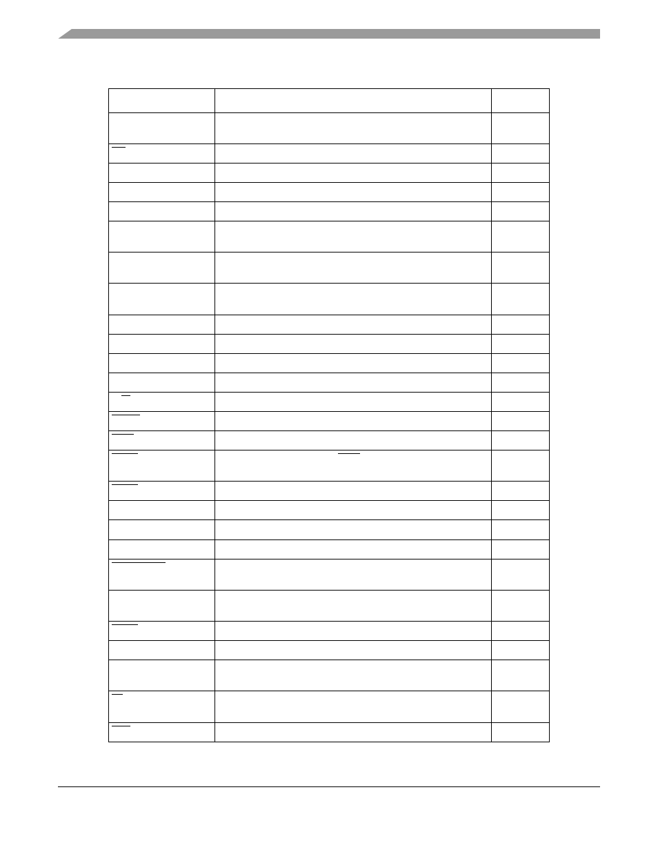
JTAG_EN
Selects between multiplexed debug module and JTAG signals at
reset.
I
OE
Indicates when an external device can drive data on the bus.
O
VDDPLL
Isolate the PLL analog circuitry from digital power supply noise.
I
VDD
Supplies positive power to the core logic and I/O pads.
I
PST[3:0]
Indicate core status.
O
VRH, VRL
High (VRH) and low (VRL) reference potentials for the analog
converter.
I
VDDA, VSSA
Isolate the QADC analog circuitry from digital power supply
noise.
I
QADC analog supply
Supplies positive power to the ESD structures in the QADC
pads.
I
QSPI_CLK
Provides the serial clock from the QSPI.
O
QSPI_CS[3:0]
Provide QSPI peripheral chip selects.
O
QSPI_DIN
Provides serial data to the QSPI.
I
QSPI_DOUT
Provides serial data from the QSPI.
O
R/W
Indicates the direction of the data transfer on the bus.
I/O
RCON
Reset configuration select.
I
RSTI
Asserted to enter reset exception processing.
I
RSTO
Automatically asserted with RSTI. Negation indicates that the
PLL has regained its lock.
O
SCAS
SDRAM synchronous column address strobe.
O
SCKE
SDRAM clock enable.
O
SCL
Clock signal for the I
2
C interface.
I/O
SDA
Data input/output for the I
2
C interface.
I/O
SDRAM_CS[1:0]
Interface to the chip-select lines of the SDRAMs within a
memory block.
O
SIZ[1:0]
Specify the data access size of the current external bus
reference.
O
SRAS
SDRAM synchronous row address strobe.
O
VSTBY
Provides standby voltage to RAM array if VDD is lost.
I
SYNCA/SYNCB
Clear the timer’s clock, providing a means of synchronization to
externally clocked or timed events.
I
TA
Indicates that the external data transfer is complete and should
be asserted for one CLKOUT cycle.
I
TEA
Indicates that an error condition exists for the bus transfer.
I
Table 14-2. MCF5282 Alphabetical Signal Index (continued)
Abbreviation
Function
I/O
MCF5282 and MCF5216 ColdFire Microcontroller User’s Manual, Rev. 3