2 destination address registers (dar0-dar3), 2 destination address registers (dar0–dar3) -6, Figure 16-4 – Motorola ColdFire MCF5281 User Manual
Page 302: Contains the address, P. 16-6, 2 destination address registers (dar0–dar3)
DMA Controller Module
16-6
Freescale Semiconductor
NOTE
The backdoor enable bit must be set in both the core and SCM in order to
enable backdoor accesses from the DMA to SRAM. See
“Memory Base Address Register (RAMBAR)
” for more details.
NOTE
Flash accesses (reads/writes) by a bus master other than the core (DMA
controller or Fast Ethernet Controller), or writes to Flash by the core during
programming, must use the backdoor Flash address of IPSBAR plus an
offset of 0x0400_0000. For example, for a DMA transfer from the first
Flash location when IPSBAR is still at its default location of 0x4000_0000,
the source register would be loaded with 0x4400_0000. Backdoor Flash
read accesses can be made with the bus master, but it takes two cycles longer
than a direct read of the Flash when using the FLASHBAR address.
16.4.2
Destination Address Registers (DAR0–DAR3)
DARn, shown in
, holds the address to which the DMA controller sends data.
Figure 16-5. Destination Address Registers (DARn)
NOTE
The DMA does not maintain coherency with the cache. Therefore, DMAs
should not transfer data to cacheable memory unless software is used to
maintain the cache coherency.
NOTE
The DMA should not be used to write data to the UART transmit FIFO in
cycle steal mode. When the UART interrupt is used as a DMA request it
does not negate fast enough to get a single transfer. The UART transmit
FIFO only has one entry so the data from the second byte would be lost.
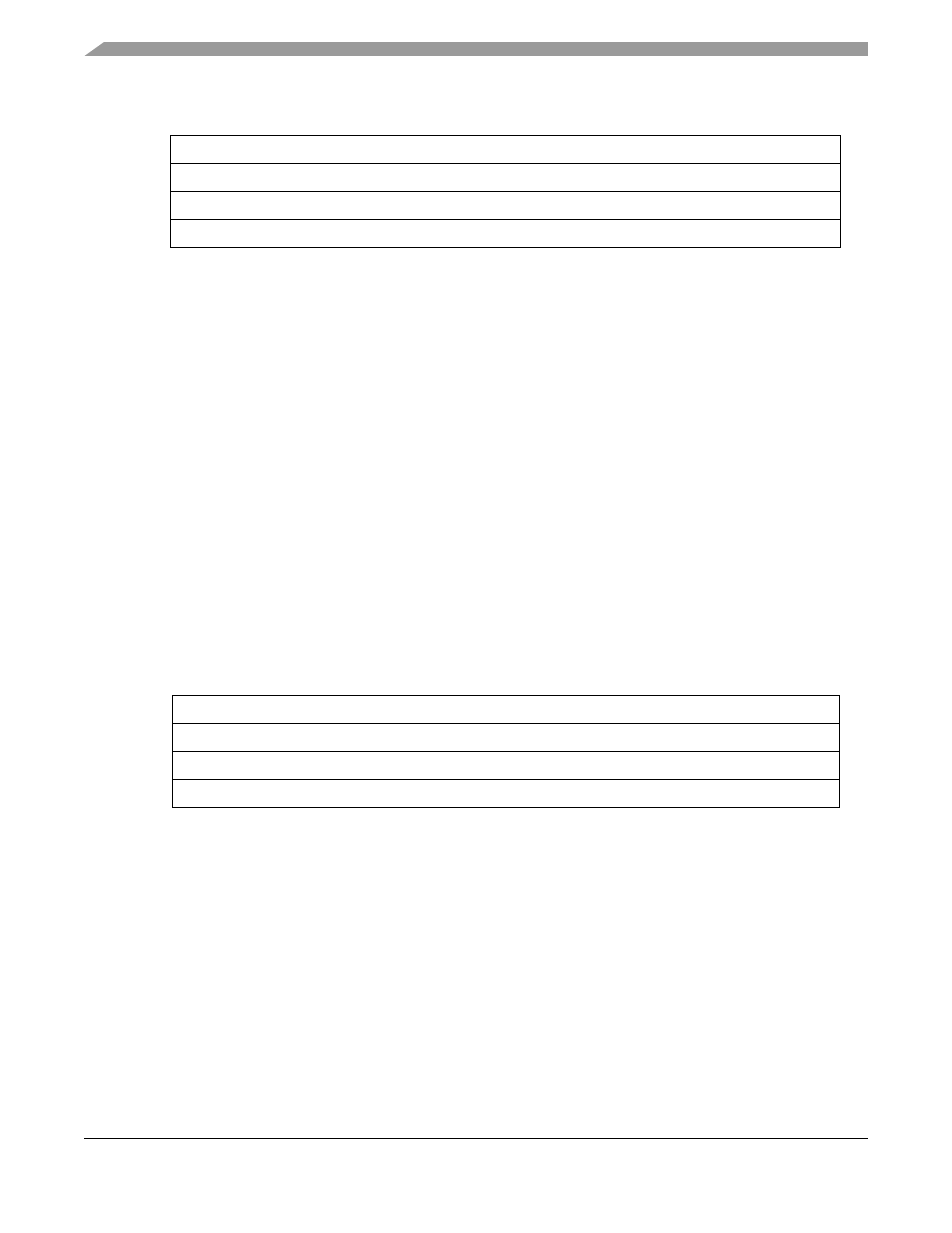
31
0
Field
SAR
Reset
0000_0000_0000_0000_0000_0000_0000_0000
R/W
R/W
Address
IPSBAR + 0x100, 0x140, 0x180, 0x1C0
Figure 16-4. Source Address Registers (SARn)
31
0
Field
DAR
Reset
0000_0000_0000_0000_0000_0000_0000_0000
R/W
R/W
Address
IPSBAR + 0x104, 0x144, 0x184, 0x1C4
MCF5282 and MCF5216 ColdFire Microcontroller User’s Manual, Rev. 3