4 dmr initialization, 4 dmr initialization -22 – Motorola ColdFire MCF5281 User Manual
Page 294
Synchronous DRAM Controller Module
15-22
Freescale Semiconductor
15.3.4
DMR Initialization
Again, in this example only the second 512-Kbyte block of each 1-Mbyte space is accessed in each bank.
In addition, the SDRAM component is mapped only to readable and writable supervisor and user data. The
DMRs have the following configuration.
With this configuration, the DMR0 = 0x0074_0075, as described in
.
3
IP
0
Indicates precharge has not been initiated.
2–0
—
Reserved. Don’t care.
31
18
17
16
Field
BAM
—
Setting
0000_0000_0111_01xx
(hex)
0 074
15
9
8
7
6
5
4
3
2
1
0
Field
—
WP
—
C/I
AM
SC
SD
UC
UD
V
Setting
xxxx_xxx0_x111_0101
(hex)
0075
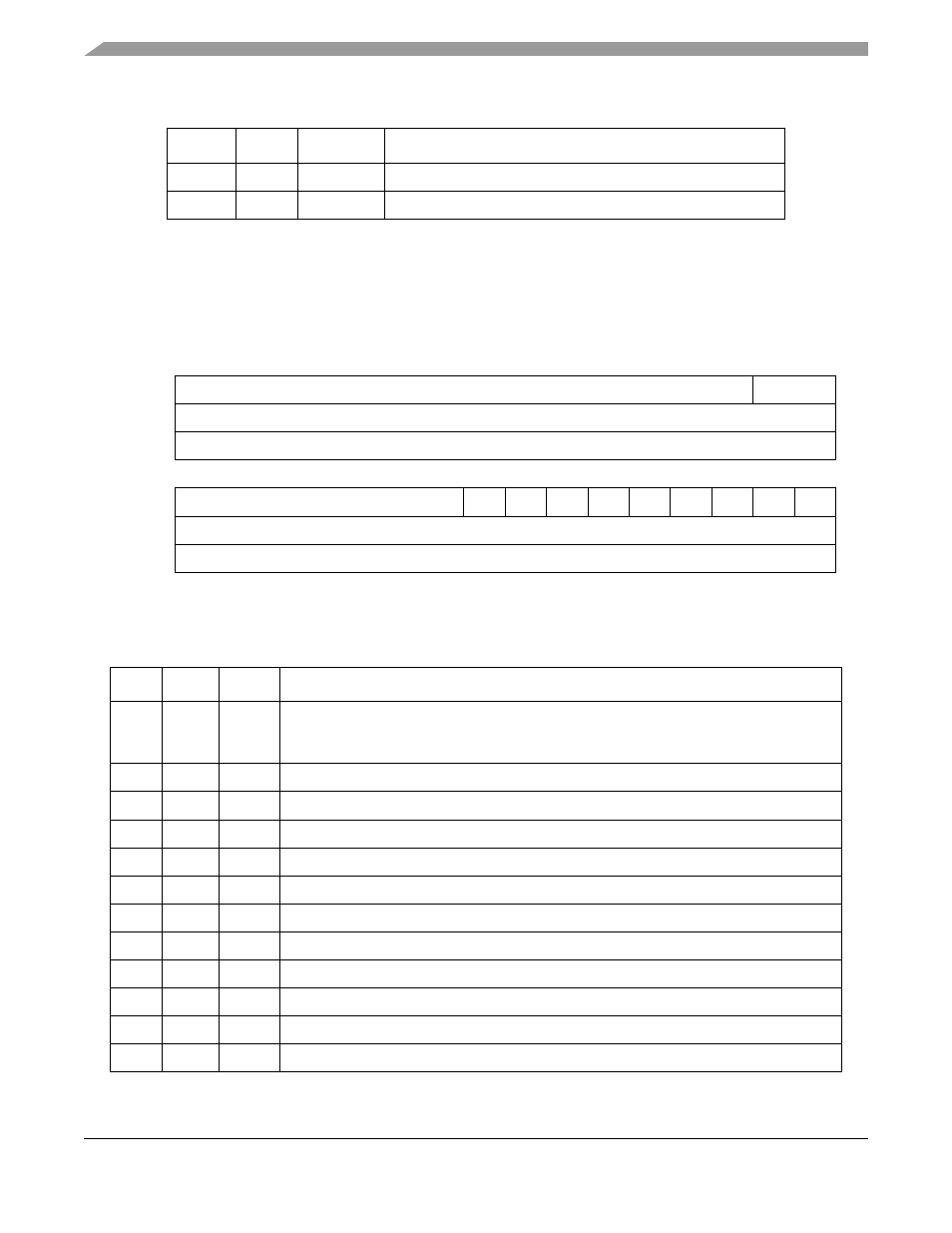
Figure 15-14. DMR0 Register
Table 15-29. DMR0 Initialization Values
Bits
Name
Setting
Description
31–18
BAM
With bits 17 and 16 as don’t cares, BAM = 0x0074, which leaves bank select bits and upper
512K select bits unmasked. Note that bits 22 and 21 are set because they are used as bank
selects; bit 20 is set because it controls the 1-Mbyte boundary address.
17–16
—
Reserved. Don’t care.
15–9
—
Reserved. Don’t care.
8
WP
0
Allow reads and writes
7
—
Reserved. Don’t care.
6
C/I
1
Disable CPU space access.
5
AM
1
Disable alternate master access.
4
SC
1
Disable supervisor code accesses.
3
SD
0
Enable supervisor data accesses.
2
UC
1
Disable user code accesses.
1
UD
0
Enable user data accesses.
0
V
1
Enable accesses.
Table 15-28. DACR Initialization Values (continued)
Bits
Name
Setting
Description
MCF5282 and MCF5216 ColdFire Microcontroller User’s Manual, Rev. 3