3 signals, 1 rsti, 2 rsto – Motorola ColdFire MCF5281 User Manual
Page 610: 4 memory map and registers, 3 signals -2, 4 memory map and registers -2
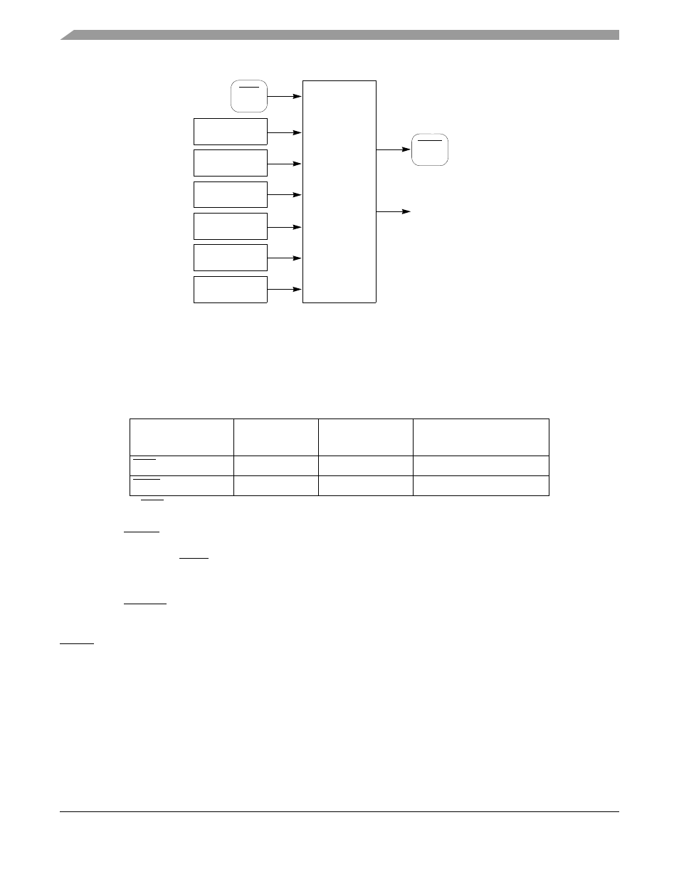
Reset Controller Module
29-2
Freescale Semiconductor
Figure 29-1. Reset Controller Block Diagram
29.3
Signals
provides a summary of the reset controller signal properties. The signals are described in the
following paragraphs.
29.3.1
RSTI
Asserting the external RSTI for at least four rising CLKOUT edges causes the external reset request to be
recognized and latched.
29.3.2
RSTO
This active-low output signal is driven low when the internal reset controller module resets the chip. When
RSTO is active, the user can drive override options on the data bus.
29.4
Memory Map and Registers
The reset controller programming model consists of these registers:
•
Reset control register (RCR), which selects reset controller functions
•
Reset status register (RSR), which reflects the state of the last reset source
See
for the memory map and the following paragraphs for a description of the registers.
Table 29-1. Reset Controller Signal Properties
Name
Direction
Input
Hysteresis
Input
Synchronization
RSTI
I
Y
Y
1
1
RSTI is always synchronized except when in low-power stop mode.
RSTO
O
—
—
Power-On
Reset
Watchdog
Timer Timeout
PLL
Loss of Clock
PLL
Loss of Lock
Software
Reset
LVD
Detect
RSTI
Pin
Reset
Controller
RSTO
Pin
To Internal Resets
MCF5282 and MCF5216 ColdFire Microcontroller User’s Manual, Rev. 3