8 port j pin assignment register (pjpar), 8 port j pin assignment register (pjpar) -20, The pjpar controls the pin function of port j – Motorola ColdFire MCF5281 User Manual
Page 520
General Purpose I/O Module
26-20
Freescale Semiconductor
26.3.2.8
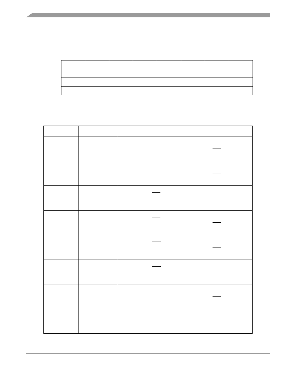
Port J Pin Assignment Register (PJPAR)
The PJPAR controls the pin function of port J.
7
6
5
4
3
2
1
0
Field
PJPA7
PJPA6
PJPA5
PJPA4
PJPA3
PJPA2
PJPA1
PJPA0
Reset
See Note 1
1
1
Reset state determined during reset configuration. PJPAn = 1 in master mode and 0 in all other modes.
R/W:
R/W
Address
IPSBAR + 0x10_0054
Figure 26-22. Port J Pin Assignment Register (PJPAR)
Table 26-12. PJPAR Field Descriptions
Bits
Name
Description
7
PJPA7
Port J pin assignment 7. This bit configures the port J7 pin for its
primary function (BS3) or digital I/O.
1 Port J7 pin configured for its primary function (BS3)
0 Port J7 pin configured for digital I/O
6
PJPA6
Port J pin assignment 6. This bit configures the port J6 pin for its
primary function (BS2) or digital I/O.
1 Port J6 pin configured for its primary function (BS2)
0 Port J6 pin configured for digital I/O
5
PJPA5
Port J pin assignment 5. This bit configures the port J5 pin for its
primary function (BS1) or digital I/O.
1 Port J5 pin configured for its primary function (BS1)
0 Port J5 pin configured for digital I/O
4
PJPA4
Port J pin assignment 4. This bit configures the port J4 pin for its
primary function (BS0) or digital I/O.
1 Port J4 pin configured for its primary function (BS0)
0 Port J4 pin configured for digital I/O
3
PJPA3
Port J pin assignment 3. This bit configures the port J3 pin for its
primary function (CS3) or digital I/O.
1 Port J3 pin configured for its primary function (CS3)
0 Port J3 pin configured for digital I/O
2
PJPA2
Port J pin assignment 2. This bit configures the port J2 pin for its
primary function (CS2) or digital I/O.
1 Port J2 pin configured for its primary function (CS2)
0 Port J2 pin configured for digital I/O
1
PJPA1
Port J pin assignment 1. This bit configures the port J1 pin for its
primary function (CS1) or digital I/O.
1 Port J1 pin configured for its primary function (CS1)
0 Port J1 pin configured for digital I/O
0
PJPA0
Port J pin assignment 0. This bit configures the port J0 pin for its
primary function (CS0) or digital I/O.
1 Port J0 pin configured for its primary function (CS0)
0 Port J0 pin configured for digital I/O
MCF5282 and MCF5216 ColdFire Microcontroller User’s Manual, Rev. 3