2 memory base address register (rambar), 2 memory base address register (rambar) -3, Section 8.4.2, “memory base address – Motorola ColdFire MCF5281 User Manual
Page 155: Register (rambar)
System Control Module (SCM)
Freescale Semiconductor
8-3
5. Chip Selects
NOTE
This is the list of memory access priorities when viewed from the processor
core.
See
and
for descriptions of the bits in IPSBAR.
8.4.2
Memory Base Address Register (RAMBAR)
The processor supports dual-ported local SRAM memory. This processor-local memory can be accessed
directly by the core and/or other system bus masters. Since this memory provides single-cycle accesses at
processor speed, it is ideal for applications where double-buffer schemes can be used to maximize
system-level performance. For example, a DMA channel in a typical double-buffer (also known as a
ping-pong scheme) application may load data into one portion of the dual-ported SRAM while the
processor is manipulating data in another portion of the SRAM. Once the processor completes the data
calculations, it begins processing the just-loaded buffer while the DMA moves out the just-calculated data
from the other buffer, and reloads the next data block into the just-freed memory region. The process
repeats with the processor and the DMA “ping-ponging” between alternate regions of the dual-ported
SRAM.
The processor design implements the dual-ported SRAM in the memory space defined by the RAMBAR
register. There are two physical copies of the RAMBAR register: one located in the processor core and
accessible only via the privileged MOVEC instruction at CPU space address 0xC05, and another located
in the SCM at IPSBAR + 0x008. ColdFire core accesses to this memory are controlled by the
processor-local copy of the RAMBAR, while module accesses are enabled by the SCM's RAMBAR.
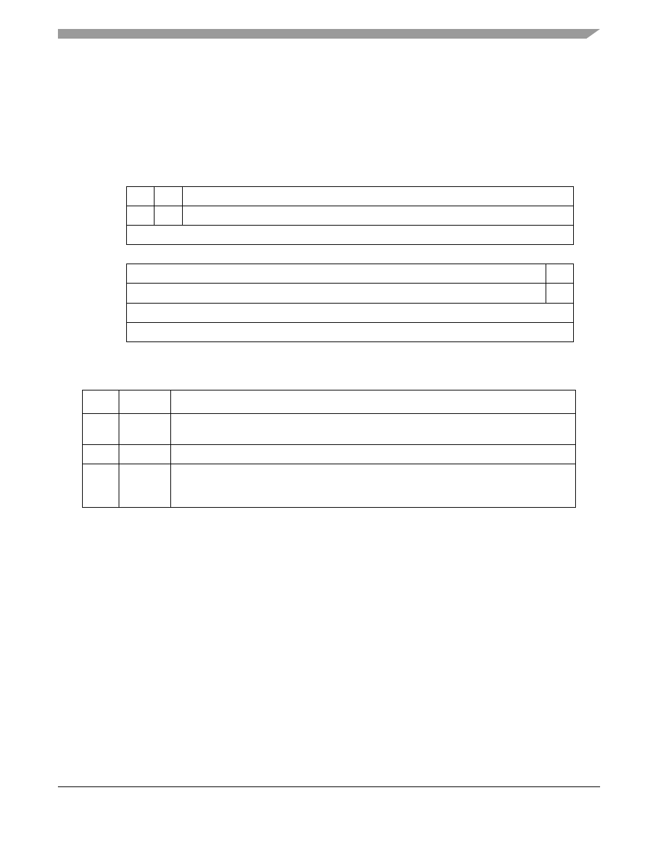
31
30
29
16
Field BA31 BA30
—
Reset
0
1
—
R/W
R/W
15
1
0
Field
—
V
Reset
—
1
R/W
R/W
Address
IPSBAR + 0x000
Figure 8-1. IPS Base Address Register (IPSBAR)
Table 8-2. IPSBAR Field Description
Bits
Name
Description
31–30
BA
Base address. Defines the base address of the 1-Gbyte internal peripheral space. This is the
starting address for the IPS registers when the valid bit is set.
29–1
—
Reserved, should be cleared.
0
V
Valid. Enables/disables the IPS Base address region. V is set at reset.
0 IPS Base address is not valid.
1 IPS Base address is valid.
MCF5282 and MCF5216 ColdFire Microcontroller User’s Manual, Rev. 3