8 external interface timing characteristics, 8 external interface timing characteristics -11, Table 33-13 – Motorola ColdFire MCF5281 User Manual
Page 695
Electrical Characteristics
Freescale Semiconductor
33-11
33.8
External Interface Timing Characteristics
lists processor bus input timings.
NOTE
All processor bus timings are synchronous; that is, input setup/hold and
output delay with respect to the rising edge of a reference clock. The
reference clock is the CLKOUT output.
All other timing relationships can be derived from these values.
Timings listed in
.
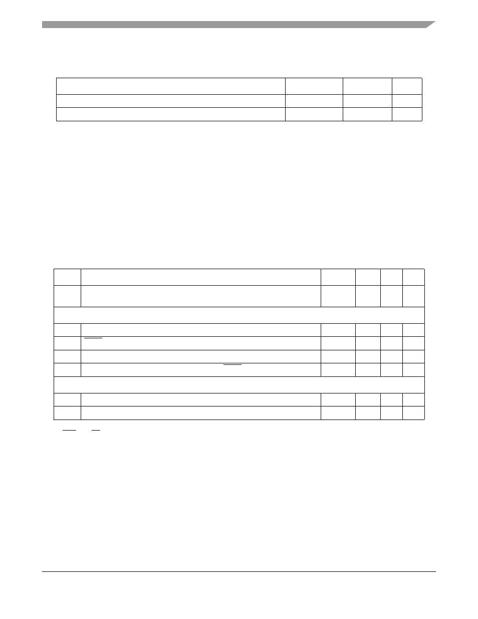
Table 33-13. SGFM Flash Module Life Characteristics
(V
DDF
= 2.7 to 3.6 V)
Parameter
Symbol
Value
Unit
Maximum number of guaranteed program/erase cycles
1
before failure
1
A program/erase cycle is defined as switching the bits from 1
→
0
→
1.
P/E
10,000
2
2
Reprogramming of a Flash array block prior to erase is not required.
Cycles
Data retention at average operating temperature of 85
°
C
Retention
10
Years
Table 33-14. Processor Bus Input Timing Specifications
Name
Characteristic
1
1
Timing specifications have been indicated taking into account the full drive strength for the pads.
Symbol
Min
Max
Unit
B0
CLKOUT — MCF521x
CLKOUT — MCF528x
t
CYC
15.15
12.5
—
ns
Control Inputs
B1a
Control input valid to CLKOUT high
2
2
TEA and TA pins are being referred to as control inputs.
t
CVCH
10
—
ns
B1b
BKPT valid to CLKOUT high
3
3
Refer to figure A-19.
t
BKVCH
10
—
ns
B2a
CLKOUT high to control inputs invalid
t
CHCII
0
—
ns
B2b
CLKOUT high to asynchronous control input BKPT invalid
3
t
BKNCH
0
—
ns
Data Inputs
B4
Data input (D[31:0]) valid to CLKOUT high
t
DIVCH
6
—
ns
B5
CLKOUT high to data input (D[31:0]) invalid
t
CHDII
0
—
ns
MCF5282 and MCF5216 ColdFire Microcontroller User’s Manual, Rev. 3