Motorola ColdFire MCF5281 User Manual
Page 279
Synchronous DRAM Controller Module
Freescale Semiconductor
15-7
10–8
CBM
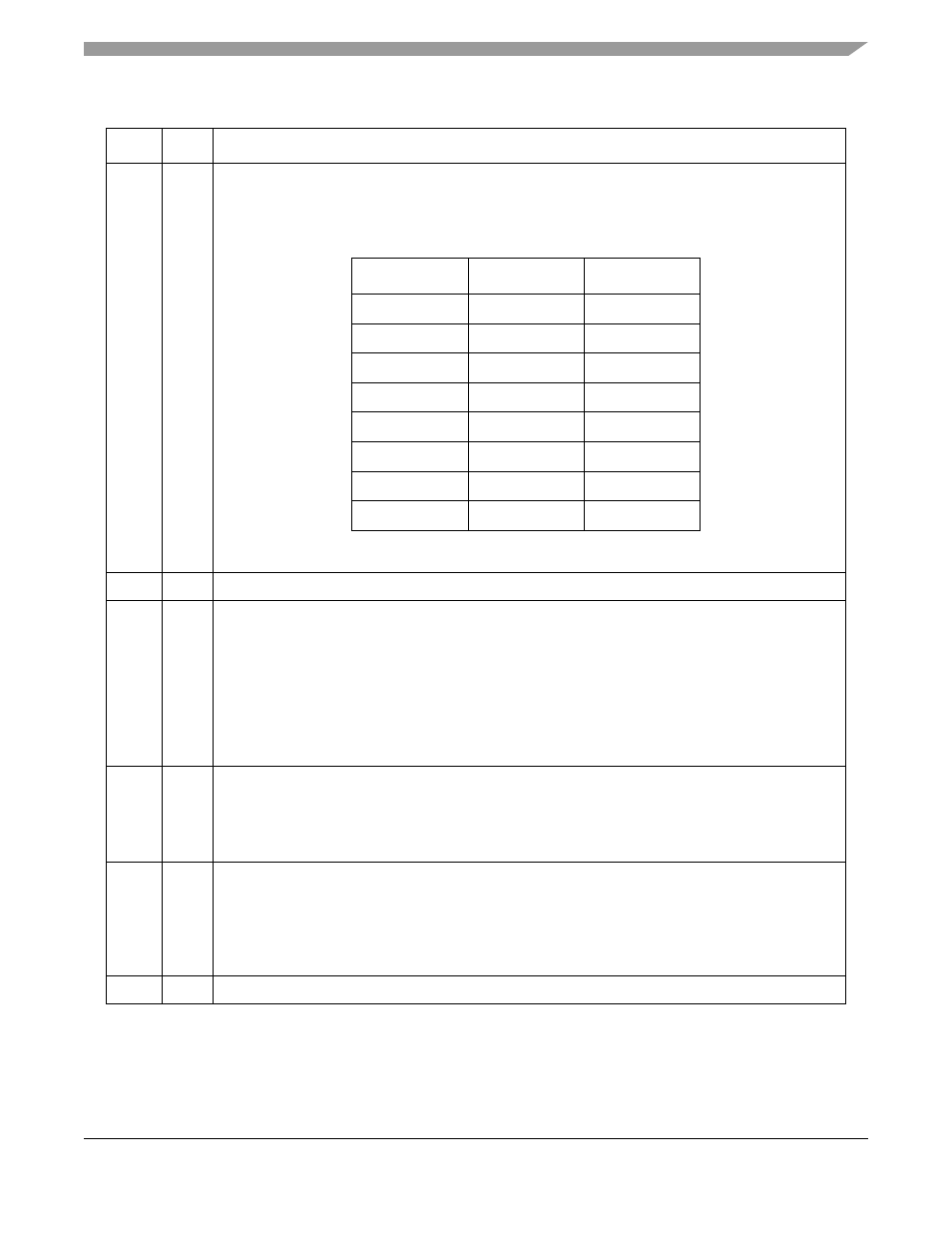
Command and bank MUX [2:0]. Because different SDRAM configurations cause the command and
bank select lines to correspond to different addresses, these resources are programmable. CBM
determines the addresses onto which these functions are multiplexed.
Note: It is important to set CBM according to the location of the command bit.
This encoding and the address multiplexing scheme handle common SDRAM organizations. Bank
select bits include a base bit and all address bits above for SDRAMs with multiple bank select bits.
7
—
Reserved, should be cleared.
6
IMRS Initiate mode register set (
MRS
) command. Setting IMRS generates a
MRS
command to the associated
SDRAMs. In initialization, IMRS should be set only after all DRAM controller registers are initialized
and
PALL
and
REFRESH
commands have been issued. After IMRS is set, the next access to an SDRAM
block programs the SDRAM’s mode register. Thus, the address of the access should be programmed
to place the correct mode information on the SDRAM address pins. Because the SDRAM does not
register this information, it doesn’t matter if the IMRS access is a read or a write or what, if any, data is
put onto the data bus. The DRAM controller clears IMRS after the
MRS
command finishes.
0 Take no action
1 Initiate
MRS
command
5–4
PS
Port size. Indicates the port size of the associated block of SDRAM, which allows for dynamic sizing of
associated SDRAM accesses. PS functions the same in asynchronous operation.
00 32-bit port
01 8-bit port
1x 16-bit port
3
IP
Initiate precharge all (
PALL
) command. The DRAM controller clears IP after the
PALL
command is
finished. Accesses via IP should be no wider than the port size programmed in PS.
0 Take no action.
1 A
PALL
command is sent to the associated SDRAM block. During initialization, this command is
executed after all DRAM controller registers are programmed. After IP is set, the next write to an
appropriate SDRAM address generates the
PALL
command to the SDRAM block.
2–0
—
Reserved, should be cleared.
Table 15-5. DACRn Field Descriptions (continued)
Bit
Name
Description
CBM
Command Bit
Bank Select Bits
000
17
18 and up
001
18
19 and up
010
19
20 and up
011
20
21 and up
100
21
22 and up
101
22
23 and up
110
23
24 and up
111
24
25 and up
MCF5282 and MCF5216 ColdFire Microcontroller User’s Manual, Rev. 3