Table 4-3 – Motorola ColdFire MCF5281 User Manual
Page 103
Cache
Freescale Semiconductor
4-5
shows the relationship between CACR[CENB, DISI, & DISD] bits and the cache configuration.
shows the relationship between CACR[DISI, DISD, INVI, & INVD] and setting the cache
invalidate all bit (CACR[CINV]).
9
DCM
Default cache mode. This bit defines the default cache mode. For more information on the selection of the effective
memory attributes, see
Section 4.3.2, “Memory Reference Attributes
0 Caching enabled
1 Caching disabled
8
DBWE
Default buffered write enable. This bit defines the default value for enabling buffered writes. If DBWE = 0, the
termination of an operand write cycle on the processor's local bus is delayed until the external bus cycle is
completed. If DBWE = 1, the write cycle on the local bus is terminated immediately and the operation buffered in the
bus controller. In this mode, operand write cycles are effectively decoupled between the processor's local bus and
the external bus. Generally, enabled buffered writes provide higher system performance but recovery from access
errors can be more difficult. For the ColdFire core, reporting access errors on operand writes is always imprecise
and enabling buffered writes further decouples the write instruction and the signaling of the fault
0 Disable buffered writes
1 Enable buffered writes
7–6
Reserved, must be cleared.
5
DWP
Default write protection
0 Read and write accesses permitted
1 Only read accesses permitted
4
EUSP
Enable user stack pointer. See
Section 2.2.3, “Supervisor/User Stack Pointers (A7 and OTHER_A7)”
for more
information on the dual stack pointer implementation.
0 Disable the processor’s use of the User Stack Pointer
1 Enable the processor’s use of the User Stack Pointer
3–2
Reserved, must be cleared.
1–0
CLNF
Cache line fill. These bits control the size of the memory request the cache issues to the bus controller for different
initial instruction line access offsets. See
for external fetch size based on miss address and CLNF.
Table 4-3. Cache Configuration as Defined by CACR
CACR
[CENB]
CACR
[DISI]
CACR
[DISD]
Configuration
Description
0
x
x
N/A
Cache is completely disabled
1
0
0
Split Instruction/
Data Cache
1 KByte direct-mapped instruction cache (uses upper
half of tag and storage arrays) and 1 KByte
direct-mapped write-through data cache (uses lower
half of tag and storage arrays)
1
0
1
Instruction Cache
2 KByte direct-mapped instruction cache (uses all of
tag and storage arrays)
1
1
0
Data Cache
2 KByte direct-mapped write-through data cache
(uses all of tag and storage arrays)
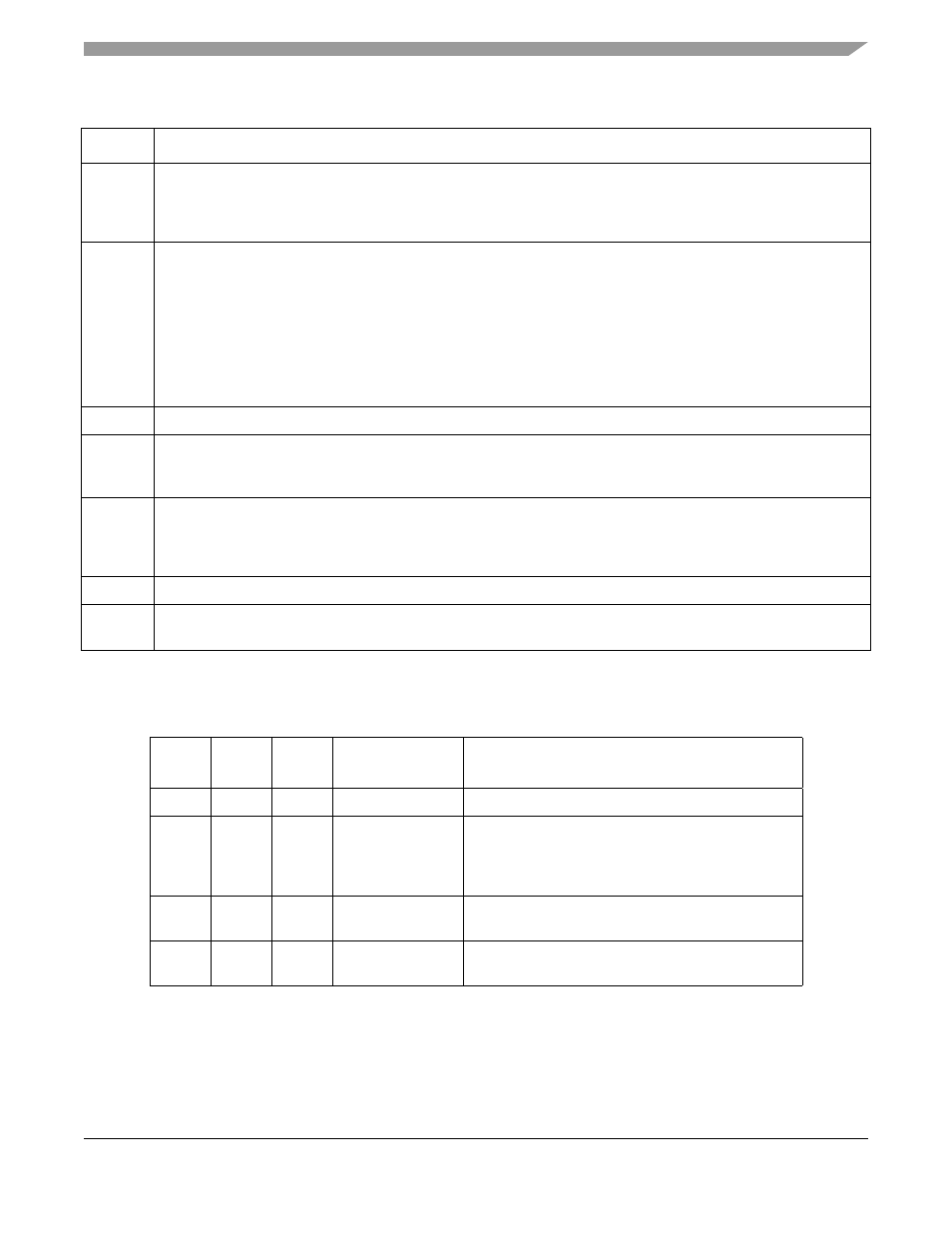
Table 4-2. CACR Field Descriptions (continued)
Field
Description
MCF5282 and MCF5216 ColdFire Microcontroller User’s Manual, Rev. 3