Motorola ColdFire MCF5281 User Manual
Page 509
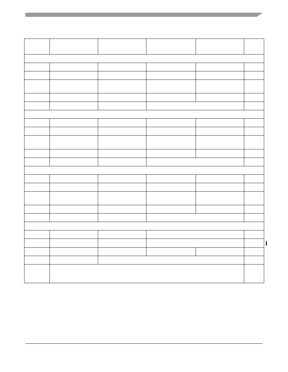
General Purpose I/O Module
Freescale Semiconductor
26-9
Port Data Direction Registers
0x10_0014
DDRA
DDRB
DDRC
DDRD
S/U
0x10_0018
DDRE
DDRF
DDRG
DDRH
S/U
0x10_001C
DDRJ
DDRDD
DDREH
(Reserved on MCF521x)
DDREL
S/U
0x10_0020
DDRAS
DDRQS
DDRSD
DDRTC
S/U
0x10_0024
DDRTD
DDRUA
Reserved
S/U
Port Pin Data/Set Data Registers
0x10_0028
PORTAP/SETA
PORTBP/SETB
PORTCP/SETC
PORTDP/SETD
S/U
0x10_002C
PORTEP/SETE
PORTFP/SETF
PORTGP/SETG
PORTHP/SETH
S/U
0x10_0030
PORTJP/SETJ
PORTDDP/SETDD
PORTEHP/SETEH
(Reserved on MCF521x)
PORTELP/SETEL
S/U
0x10_0034
PORTASP/SETAS
PORTQSP/SETQS
PORTSDP/SETSD
PORTTCP/SETTC
S/U
0x10_0038
PORTTDP/SETTD
PORTUAP/SETUA
Reserved
S/U
Port Clear Output Data Registers
0x10_003C
CLRA
CLRB
CLRC
CLRD
S/U
0x10_0040
CLRE
CLRF
CLRG
CLRH
S/U
0x10_0044
CLRJ
CLRDD
CLREH
(Reserved on MCF521x)
CLREL
S/U
0x10_0048
CLRAS
CLRQS
CLRSD
CLRTC
S/U
0x10_004C
CLRTD
CLRUA
Reserved
S/U
Port Pin Assignment Registers
0x10_0050
PBCDPAR
PFPAR
PEPAR
S/U
0x10_0054
PJPAR
PSDPAR
PASPAR
S/U
0x10_0058
PEHLPAR
PQSPAR
PTCPAR
PTDPAR
S/U
0x10_005C
PUAPAR
Reserved
S/U
0x10_0060
–
0x10_007C
Reserved
1
S/U = supervisor or user mode access. User mode accesses to supervisor-only addresses have no effect and cause a cycle
termination transfer error.
2
Writing to reserved address locations has no effect and reading returns 0s.
Table 26-2. Ports Module Memory Map (continued)
IPSBAR +
Offset
31–24
23–16
15–8
7–0
Access
1
MCF5282 and MCF5216 ColdFire Microcontroller User’s Manual, Rev. 3