Table 26-10 – Motorola ColdFire MCF5281 User Manual
Page 518
General Purpose I/O Module
26-18
Freescale Semiconductor
The reset values for all bits and fields in PEPAR are shown in
6
PEPA3
Port E pin assignment 3
This bit configures the port E3 pin for its alternate function
(SYNCA) or digital I/O.
1 Port E3 pin configured for alternate function (SYNCA)
0 Port E3 pin configured for digital I/O
NOTE: The SIZ1 primary function on the port E3 pin is enabled by
the SZEN bit in the CCR register. Please refer to the
“Chip Configuration Module (CCM)
for more information on chip
configuration and the SZEN bit.
4
PEPA2
Port E pin assignment 2
This bit configures the port E2 pin for its alternate function
(SYNCB) or digital I/O.
1 Port E2 pin configured for alternate function (SYNCB)
0 Port E2 pin configured for digital I/O
NOTE: The SIZ0 primary function on the port E2 pin is enabled by
the SZEN bit in the CCR register. Please refer to the
“Chip Configuration Module (CCM)
,” for more information on chip
configuration and the SZEN bit.
3–2
PEPA1
Port E pin assignment 1.
This two-bit field in PEPAR[3:2] configures the port E1 pin for its
primary function (TS), alternate function (SYNCA), or digital I/O.
0x Port E1 pin configured for digital I/O
10 Port E1 pin configured for alternate function (SYNCA)
11 Port E1 pin configured for primary function (TS)
1-0
PEPA0
Port E pin assignment 0.
This two-bit field in PEPAR[1:0] configures the port E0 pin for its
primary function (TIP), alternate function (SYNCB), or digital I/O.
0x Port E0 pin configured for digital I/O
10 Port E0 pin configured for alternate function (SYNCB)
11 Port E0 pin configured for primary function (TIP)
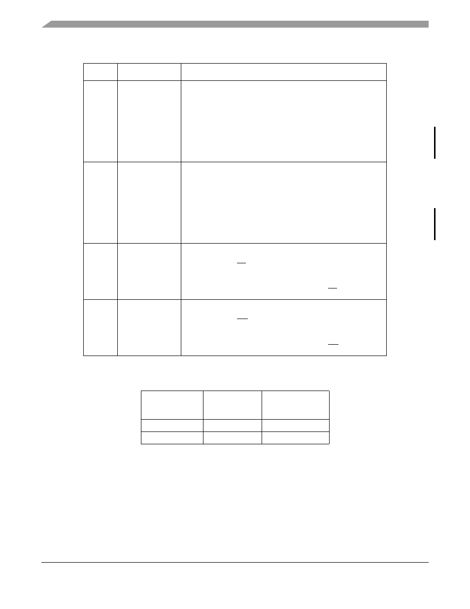
Table 26-10. Reset Values for PEPAR Bits and Fields
Mode of
Operation
Reset Values
for PEPAn Bits
(n = 2,3,4,5,6,7)
Reset Values for
PEPAn Fields
(n = 0,1)
Master mode
1
11
Single chip mode
0
00
Table 26-9. PEPAR Field Descriptions (continued)
Bits Name
Description
MCF5282 and MCF5216 ColdFire Microcontroller User’s Manual, Rev. 3