5 initialization/application information, 5 initialization/application information -28 – Motorola ColdFire MCF5281 User Manual
Page 528
General Purpose I/O Module
26-28
Freescale Semiconductor
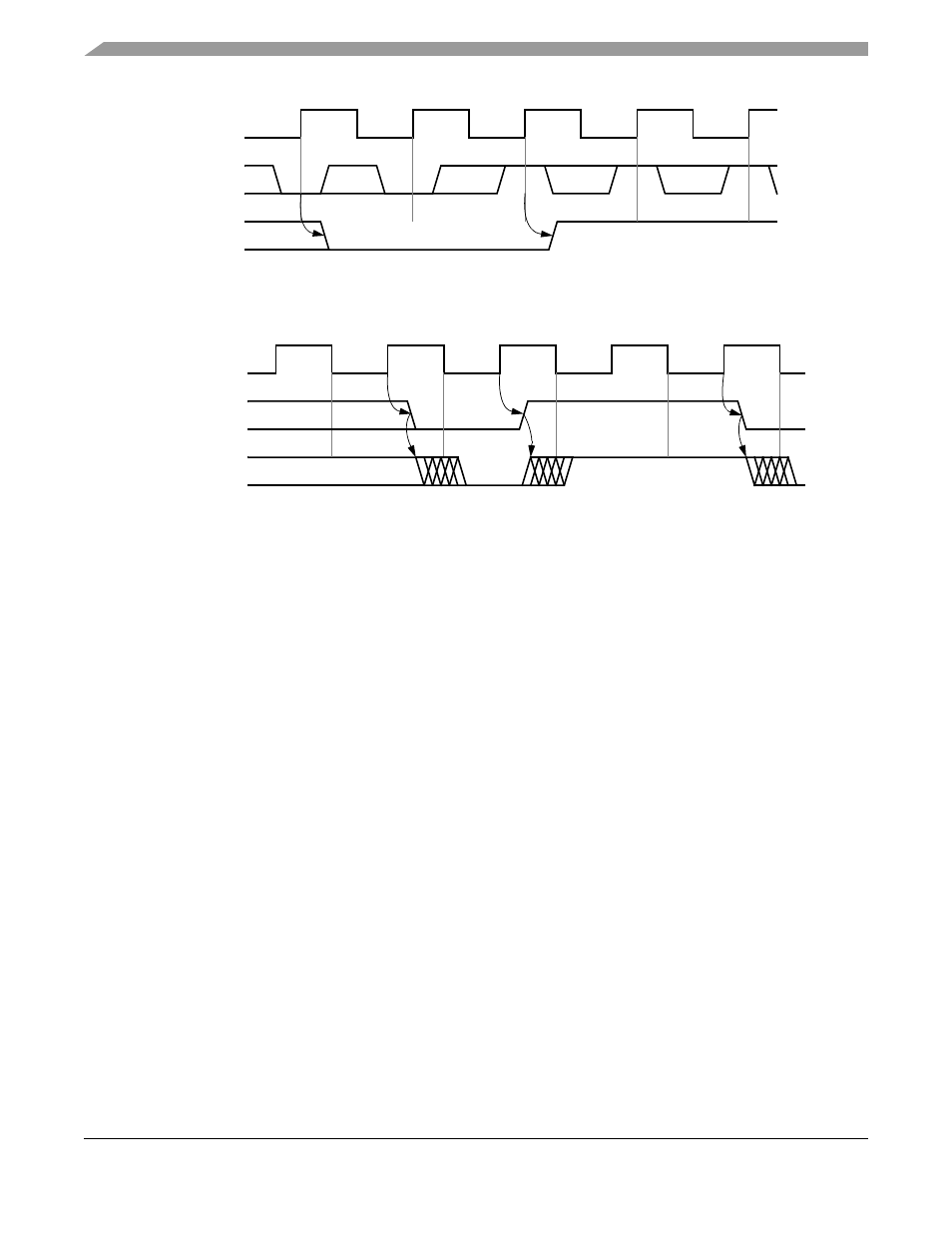
Figure 26-30. Digital Input Timing
Data written to the PORTn register of any pin configured as a digital output is immediately driven to its
respective pin, as shown in
Figure 26-31. Digital Output Timing
26.5
Initialization/Application Information
The initialization for the ports module is done during reset configuration. Some of the registers are reset
to a predetermined state, and others are reset according to which mode of operation is chosen by reset
configuration. Refer to
Section 26.3, “Memory Map/Register Definition
,” for more details on reset and
initialization.
CLKOUT
PIN DATA
INPUT
REGISTER
PIN
CLKOUT
OUTPUT DATA
OUTPUT PIN
REGISTER
MCF5282 and MCF5216 ColdFire Microcontroller User’s Manual, Rev. 3