3 logic blocks, 1 logic blocks overview, 2 transmission principle between tsip and serdes – Artesyn ATCA-8310 Installation and Use (May 2014) User Manual
Page 434: Figure 8-13, Logic blocks overview, Cpld and fpga
CPLD and FPGA
ATCA-8310 Installation and Use (6806800M72E)
434
8.4.3
Logic Blocks
8.4.3.1
Logic blocks Overview
8.4.3.2
Transmission principle between TSIP and SERDES
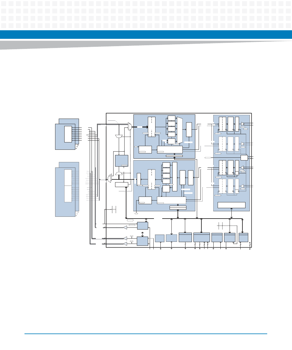
The DSP FPGA uses the Generic 8B10B mode of the flexiPCS (Physical Coding Sublayer) block
of the Lattice SC/M FPGA device to transfer the speech information of up to 60 TSIP each with
32.758 MBit/s (512 Channels) to and from the RTM FPGA. 4096 sample speech information of
60 TSIP channels (245760 bits) equals to one 125 μs frame together with 16 bit supplementary
information and 32 bit CRC frame checksum are transferred as a packet across one 2.5 Gbit/s
Figure 8-13 Logic blocks overview
Current DSP
Pool
P/S
SER(15..0)
REF
REF
FB
CLK32M
FS_A
FS_B
TELCO_
CLK_
32M768
SerDes
Control/Status
Register
125 MHz
FS_A
32.768 MHz
Mux & Transmit Control
FS_A
Data
S/P
Reg
(16:240)
Slow Register
Control
Pay-
load
Out
Reg
(x60)
32.768 MHz
FS_B
FS_B
125 MHz
PD
TELCO_
CLK_8K
DeMUX & Receive Control
FSGEN
SPI-Slave
to Wishbone
CLK
MOSI
MISO
CS
DSP Power Control
8b10b
Encode
CRC
Gen
Phase
Comp.
FIFO
Phase
Comp.
FIFO
S/P
10b8b
Decode
TX_K(1:0)
Wishbone
to I2C
Bridge
SCL
SDA
Error Counter
HS_TX1_P
HS_TX1_N
HS_RX1_P
HS_RX1_N
GCLK
32.768 MHz
CLKA(0..9)
CLKB(0..9)
FS_B(0..9)
Suppl.
Reg (x16)
125 MHz
Payload
Exp Reg0
(x60)
Wishbone Bus
FS
Suppl.
Reg
(x16)
Com-
pression
FIFO
(x60)
Receive Pattern Reg
P/S
125 MHz
8b10b
Encode
Phase
Comp.
FIFO
F
m
a
HS_TX2_P
HS_TX2_N
Reference
Clock
PLL
RX_K(1:0)
RX_CRC_ERR
DES(15..0)
125 MHz
Phase
Comp.
FIFO
S/P
10b8b
Decode
F
m
F
a
HS_RX2_P
HS_RX2_N
1. 25 GHz
1. 25 GHz
2.5 GHz
31
DSP Reset and NMI
1
5
TX(19..0)
4
from
Base Board
and DSP
Module
SERDES_CLK125 M
DSP Status and
Interrupt
40
CLKGEN
125 MHz
Re-
covery
ITU-T O.150
PSR-Generator
and
Comparator
TX(59..0)
Control, Result
21
10
10
DES2TSIP
Data
MUX
(240 :16)
TSIP2SER
SERDES
32.768 MHz
125 MHz
32.768 MHz
Transmit Pattern Reg
Re
s
u
lt
CLK_FB
BaseID and
SubmodID
Register
Register
Register
Register
to DSP-
Module
to Host
2
1
from
Base
Board
from
DSP
Module
to DSP-
Module
to
Base
Board
4
Reserved
Re-
covery
Pattern
FS_A (9..0)
FS_B(9..0)
CLK_A(9..0)
CLK_B(9..0)
TR(19..10)
TX(9..0)
TX(19..10)
TR(19..10)
1024
Time
Slots
DSP (Current type)
0
9
TR(19..0)
FS_B(0..11)
CLK_A(0..11)
CLK_B(0..11)
TX1(0..11)
TR0(0..11)
TR1(0..11)
Preparation
DSP (New type)
FS_A (11..0)
FS_B(11..0)
CLK_A(11..0)
CLK_B(11..0)
TX0(11..0)
TX1(23..12)
TR0(11..0)
TR1(11..0)
TX1(35..24)
TR0(47..36)
TR1(47..36)
FS_B(23..12)
CLK_A(23..12)
CLK_B(23..12)
0
11
TX(47..0)
TR(47..0)
TX0(35..24)
FS_A(23..12)
TX1
TX0
TR1
TR0
TSIP
TX1
TX0
TR1
TR0
TSIP0
TX1
TX0
TR1
TR0
TSIP1
1024
Time
Slots
1024
Time
Slots
FS_A(0..9)
O
th
er
In
te
rn
al
so
ur
ce
s
M
ai
n
in
te
rn
al
cl
oc
k
1.25 GHz
/
2.5 GHz
1.25 GHz
/
Status and
Interrupt
Register
from DSP-
Module
to Host
TX(59..48)
Spare
TR(59..48)
Spare
TR
(5
9
..
1
)
DES(7..0)
DES(15..8)
SER(7..0)
SER(15..8)
Payload
Exp Reg0
(x60)
Payload
Exp Reg0
(x60)
Payload
Exp Reg0
(x60)
Payload
Trf Reg0
(x60)
Payload
Trf Reg0
(x60)
Payload
Trf Reg0
(x60)
125 MHz
125 MHz
Payload
Trf Reg0
(x60)
TX_CRC_INIT
TX_K
CRC
Check
32.768 MHz
Slow Register
Control
32.768 MHz
16 Bit
Aligner
RX_CRC_INIT
TX_K
125 MHz
RX_K
DeCom-
pression
FIFO
(x60)
125 MHz
32.768 MHz
M
U
X
M
U
X
M
U
X
M
U
X
M
U
X
TX(59..48)
Spare
M
U
X