Table 8-164, Dmc 2 spi ls word data register, Table 8-165 – Artesyn ATCA-8310 Installation and Use (May 2014) User Manual
Page 349: Dmc 2 spi ms word data register, Table 8-166, Artm spi access control register, Cpld and fpga, 40 artm spi access registers
CPLD and FPGA
ATCA-8310 Installation and Use (6806800M72E)
349
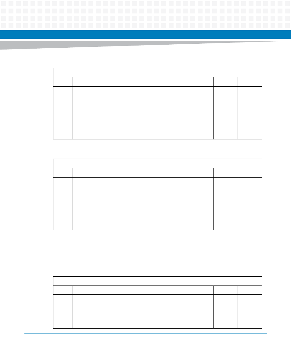
8.2.2.3.40 ARTM SPI Access Registers
Table 8-164 DMC 2 SPI LS Word Data Register
Address: 0xCA - 0xCB
Bit Description
Default
Access
15:0
DMC 2 SPI LS Word Write Data Register.
Contains the write bits 15:0 for a DMC register write access
-
SPP: w
DMC 2 SPI LS Word Read Data Register.
Contains the data bits 15:0 of the selected DMC 32 bit register
when the DMC SPI access has terminated successfully.
Note: Read DMC 2 SPI LS Word Data Register content as long SPI
access not started.
0
SPP: r
Table 8-165 DMC 2 SPI MS Word Data Register
Address: 0xCC -0xCD
Bit Description
Default
Access
15:0
DMC 2 SPI MS Word Write Data Register.
Contains the write bits 31:16 for a DMC register write access
-
SPP: w
DMC 2 SPI MS Word Read Data Register.
Contains the data bits 31:16 of the selected DMC 32 bit register
when the DMC SPI access has terminated successfully.
Note: Read DMC 2 SPI MS Word Data Register content as long SPI
access not started.
0
SPP: r
Table 8-166 ARTM SPI Access Control Register
Address: 0xD0
Bit Description
Default
Access
5:0
ARTM SPI Address. (up to 64 bytes)
0
SPP: r/w
6
SPI Busy Bit:
0: Ready for next read or write access
1: Busy. The SPI clock is still toggling.
0
SPP: r