Table 8-70, Spp boot bank selection, Cpld and fpga – Artesyn ATCA-8310 Installation and Use (May 2014) User Manual
Page 298: 6 spp boot bank selection
CPLD and FPGA
ATCA-8310 Installation and Use (6806800M72E)
298
8.2.2.3.6 SPP Boot Bank Selection
15:8
Inverted level of Switch Signals SW_[7:0]
Bit 0: SW5 Pin 1
Bit 1: SW5 Pin 2
Bit 2: SW5 Pin 3
Bit 3: SW5 Pin 4
Bit 4: SW6 Pin 1
Bit 5: SW6 Pin 2
Bit 6: SW6 Pin 3
Bit 7: SW6 Pin 4
Note: The default values may be overwritten by SPP write access.
Ext.
SW_[7:0]
SPP: r/w
Table 8-69 Status Register (continued)
Address: 0x06 - 0x07
Bit Description
Default
Access
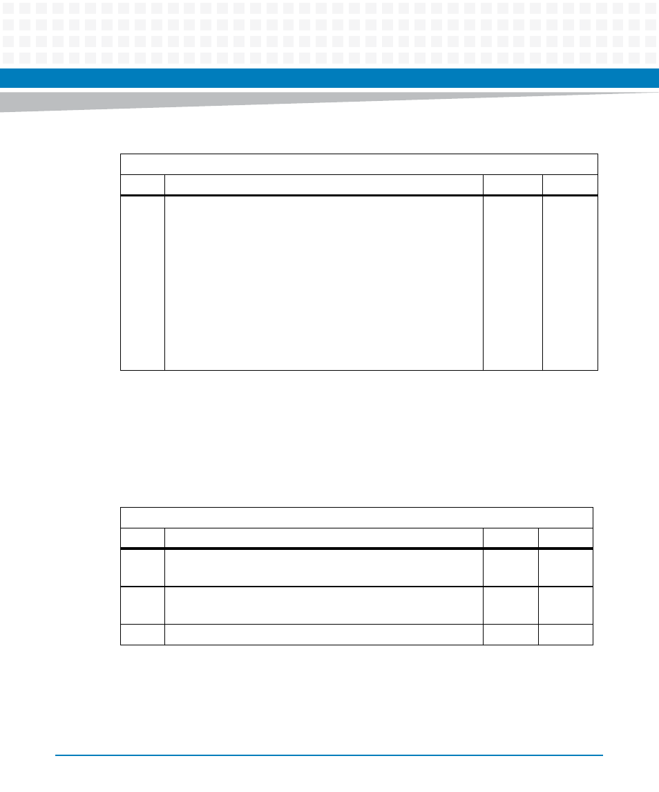
Table 8-70 SPP Boot Bank Selection
Address: 0x08
Bit Description
Default
Access
0
SPP Current Selected Bank.
Latched signal SPP_FLASH_SEL with rising edge of SPP_HRESET_
Ext.
r
1
SPP Selected Bank.
Level of signal SPP_FLASH_SEL
Ext.
r
7:2
Reserved
0
r
This manual is related to the following products:
See also other documents in the category Artesyn Equipment:
- ARTM-9405 16x10GbE Installation and Use Guide (May 2014) (64 pages)
- ATCA 7370 / ATCA 7370-S Installation and Use (January 2015) (256 pages)
- ATCA 7370 / ATCA 7370-S Installation and Use (September 2014) (254 pages)
- ARTM-831X Installation and Use (June 2014) (346 pages)
- ATCA-7350 - Integrating with Workbench User Guide (September 2014) (34 pages)
- ATCA-7350 Installation and Use (September 2014) (208 pages)
- ATCA-7365-CE Installation and Use (May 2014) (306 pages)
- ATCA-7365-CE Installation and Use (Jan 2015) (300 pages)
- ATCA-7365-CE Installation and Use (May 2014) (294 pages)
- ATCA-7368 Installation and Use (June 2014) (222 pages)
- ATCA-7475 Installation and Use (October 2014) (284 pages)
- ATCA-7480 Installation and Use (April 2015) (330 pages)
- ATCA-8330 Installation and Use (April 2015) (236 pages)
- ATCA-9305 User's Manual (May 2014) (270 pages)
- ATCA-9405 Installation and Use (October 2014) (168 pages)
- ATCA-F120 Installation and Use (August 2014) (122 pages)
- ATCA-F140 Installation and Use (September 2014) (138 pages)
- ATCA-MF106 Installation and Use (September 2014) (86 pages)
- Centellis-4440/AXP1440 Installation and Use (September 2014) (208 pages)
- Centellis 4410 (AXP-1410) Installation and Use (July 2014) (202 pages)
- Centellis 2100 Release 3.0 Installation and Use (March 2015) (176 pages)
- Centellis 2100 Release 3.0 Installation and Use (March 2015) (192 pages)
- Centellis 2000 User Card-10GE Installation and Use (May 2014) (54 pages)
- Centellis 2000 User Card-10GE with Telco Alarm Installation and Use (May 2014) (60 pages)
- COMX-CAR-210 Installation and Use (August 2014) (76 pages)
- COMX-P1022 Installation and Use (July 2014) (84 pages)
- COMX-P2020 Installation and Use (February 2015) (100 pages)
- COMX-CORE Series Installation and Use (August 2014) (128 pages)
- COMX-P2020 Installation and Use (July 2014) (100 pages)
- COMX-P4080-2G-ENP2 Installation and Use (August 2014) (70 pages)
- COMX-P4080 Installation and Use (August 2014) (126 pages)
- COMX-P40x0 ENP2 Installation and Use (August 2014) (130 pages)
- COMX-P40x0 ENP2 Installation and Use (January 2015) (140 pages)
- iVPX7225 RTM Installation and Use (April 2015) (56 pages)
- MITX-430/MITX-440-DVI-2E Installation and Use (August 2014) (118 pages)
- CPCI-6200 Installation and Use (May 2015) (234 pages)
- SCP-MITX-CORE-820-SM Installation and Use (August 2014) (132 pages)
- iVPX7225 Installation and Use (April 2015) (168 pages)
- MVME2502 Installation and Use (August 2014) (150 pages)
- MVME2502 Installation and Use (December 2014) (166 pages)
- MVME2500 VxWorks 6.8 AMP User Guide (August 2014) (40 pages)
- MVME2500 VxWorks 6.8 User Guide (April 2014) (44 pages)
- MVME3100 Single Board Computer Installation and Use (June 2014) (156 pages)
- MVME4100 Single Board Computer Installation and Use (June 2014) (136 pages)