Cpld and fpga – Artesyn ATCA-8310 Installation and Use (May 2014) User Manual
Page 293
CPLD and FPGA
ATCA-8310 Installation and Use (6806800M72E)
293
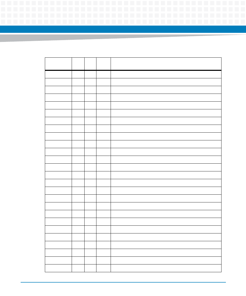
0x18 - 0x1B
x
x
GPP/SPP Watchdog Registers
0x1C - 0x1F
x
x
Real Time Clock Register
0x20 - 0x33
x
GPP Interrupt Registers
0x40
x
x
Mailbox output 1. See chapter
0x41
x
x
Mailbox Input 1 from opposite CPU. See chapter
0x42
x
x
Mailbox output 2.
0x43
x
x
Mailbox Input 2 from opposite CPU.
0x44
x
x
Mailbox output 3.
0x45
x
x
Mailbox Input 3 from opposite CPU.
0x46
x
x
Mailbox output 4.
0x47
x
x
Mailbox Input 4 from opposite CPU.
0x48
x
x
Page Pointer 1 to Shared Memory
0x49
x
x
Page Pointer 2 to Shared Memory
0x4A - 0x4D
x
x
Semaphore Registers 1 to 4
0x50 - 0x57
x
x
Shared Memory 8 byte Area. Page 1
0x58 - 0x5F
x
x
Shared Memory 8 byte Area. Page 2
0x60 - 0x6F
x
x
Telecom Clocking Registers
0x70
x
x
Test Control and Status Register
0x71
x
x
Force CRC Error Register
0x72 - 0x73
x
Glue Logic FPGA Code SPI Update Registers
0x74 - 0x75
x
x
x
SPP Persistent Memory Registers
0x7C
x
x
x
SPP Scratch Register
0x7D
x
x
x
GPP Scratch Register
0x7E
x
x
x
IPMC Scratch Register
0x7F
x
-
x
SPP and IPMC access to GPP Port 80
0x80 - 0x89
x
NA
NA
Failover Status/Control Registers
Table 8-64 Glue FPGA Register Overview (continued)
Address /
Range
SPP
GPP
IPMC
Description