2 registers, Table 8-26, Register default – Artesyn ATCA-8310 Installation and Use (May 2014) User Manual
Page 264: Table 8-27, Register access type, Cpld and fpga
CPLD and FPGA
ATCA-8310 Installation and Use (6806800M72E)
264
8.2.2
Registers
For register description, the convention shown in
, and
.
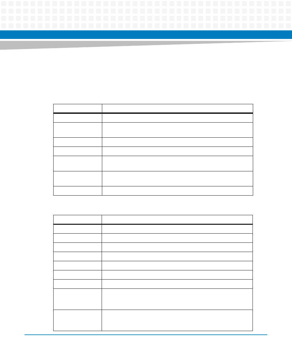
Table 8-26 Register Default
Default
Description
-
Not applicable or undefined
0 or 1
Default value after PWR_GOOD is valid or after global reset
deassertion.
Undef.
Undefined value
Default value after deassertion of the reset signal
PWR_GOOD: 0 or 1
Default value after PWR_GOOD is valid. Any other reset source don't
modify the register content
SPP: 0 or 1
Default value after PWR_GOOD is valid or after SPP reset. A GPP reset
don't modify the register content
Ext.
External Reset Source. Default depends on external logic level.
Table 8-27 Register Access Type
Access
Description
r
Read only
w
Write only
r/w
Read and write
w1c
Write-1-to-clear, ignore bit while reading
r/w1c
Read and write-1-to-clear, write 0 has no effect
r/w1s
Read and write-1-to-set, write 0 has no effect
r/w1t
Read and write-1-to-toggle, write 0 has no effect
GPP:
The prefix "GPP:" signals that the access is restricted to the GPP LPC
interface. E. g.: GPP: r/w means that the register bit is read/writable
from the GPP LPC interface
SPP:
The prefix "SPP:" signals that the access is restricted to the SPP Local Bus
interface. E. g.: SPP: r/w means that the register bit is read/writable
from the SPP Local Bus interface.