Table 8-71, Gpp boot bank selection, Table 8-72 – Artesyn ATCA-8310 Installation and Use (May 2014) User Manual
Page 299: Cpld spi access control register, Cpld and fpga
CPLD and FPGA
ATCA-8310 Installation and Use (6806800M72E)
299
8.2.2.3.7 GPP Boot Bank Selection
8.2.2.3.8 CPLD SPI Access Registers
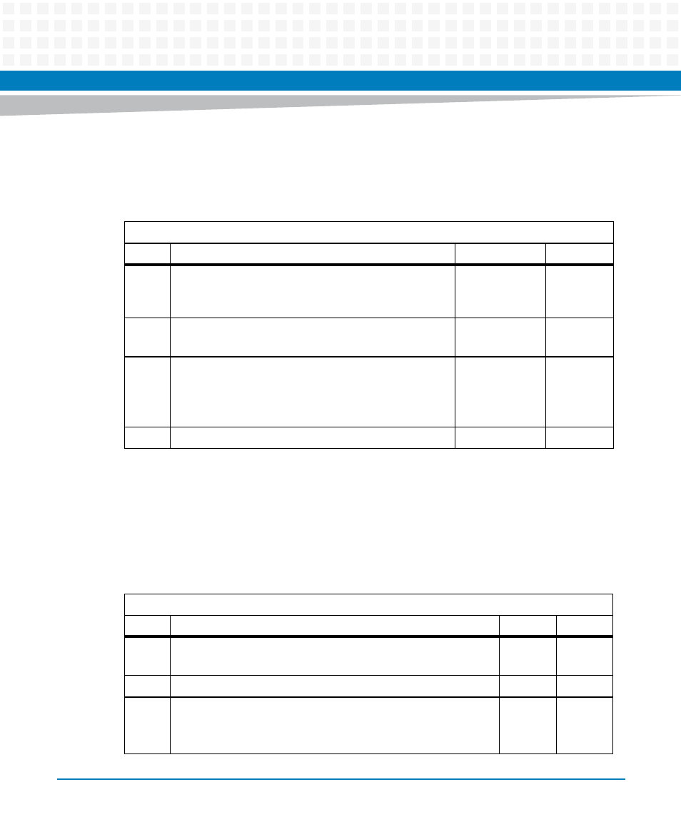
Table 8-71 GPP Boot Bank Selection
Address: 0x09
Bit Description
Default
Access
0
GPP Current Selected Bank.
Latched signal GPP_FLASH_SEL with rising edge of
GPP_HRESET_
Ext.
r
1
GPP Selected Bank.
Level of signal GPP_FLASH_SEL
Ext.
r
2
GPP Select Request. GPP request for boot bank switch
PWR_GOOD:0
SPP: r/w1s
IPMC:
r/w0c
GPP: r/w1s
7:3
Reserved
0
r
Table 8-72 CPLD SPI Access Control Register
Address: 0x0A
Bit Description
Default
Access
4:0
CPLD SPI Address. (32 bytes)
1
SPP: r/w
GPP: r/w
5
Reserved
0
r
6
SPI Busy Bit:
0: Ready for next read or write access
1: Busy. The SPI clock is still toggling. Or SPI owned by other CPU.
0
SPP: r
GPP: r
This manual is related to the following products: