Table 8-44, Logical device common decode ranges, Table 8-42 – Artesyn ATCA-8310 Installation and Use (May 2014) User Manual
Page 273: Logical device base io address msb register, Table 8-43, Logical device base io address lsb register, Cpld and fpga
CPLD and FPGA
ATCA-8310 Installation and Use (6806800M72E)
273
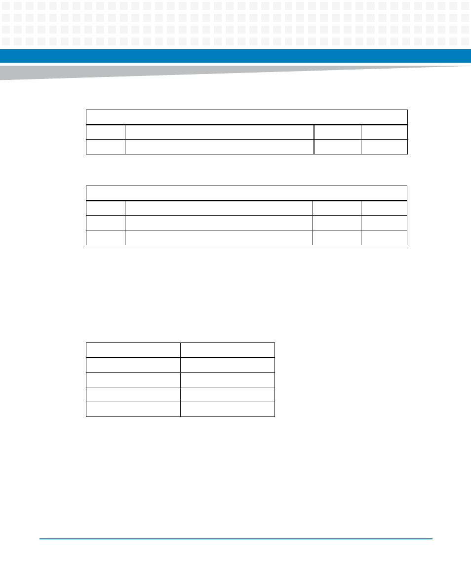
Registers 0x60 (MSB) and 0x61 (LSB) set the Logical Device Base IO for this logical device. For
example for Base IO address 0x3F8 the content of Register 0x60 is 0x03 and the content of
Register 0x61is 0xF8.
See table below for Common Decode Ranges:
Table 8-42 Logical Device Base IO Address MSB Register
Index Address: 0x60
Bit
Description
Default
Access
7:0
Logical Device Base IO Address MSB
0
GPP: r/w
Table 8-43 Logical Device Base IO Address LSB Register
Index Address: 0x61
Bit
Description
Default
Access
2:0
Bits 0 to 2 are read only. Decode is on 8 Byte boundary. 0
GPP: r
7:3
Logical Device Base IO Address LSB. (Bits 3 to 7)
0
GPP: r/w
Table 8-44 Logical Device Common Decode Ranges
IO Address range
Description
0x3F8 - 0x3FF
COM1
0x2F8 - 0x2FF
COM2
0x2E8 - 0x2EF
COM3
0x3E8 - 0x3EF
COM4