1 cpld register overview, Table 8-2, Register access type – Artesyn ATCA-8310 Installation and Use (May 2014) User Manual
Page 247: Table 8-3, Cpld register overview, Cpld and fpga
CPLD and FPGA
ATCA-8310 Installation and Use (6806800M72E)
247
8.1.2.1
CPLD Register Overview
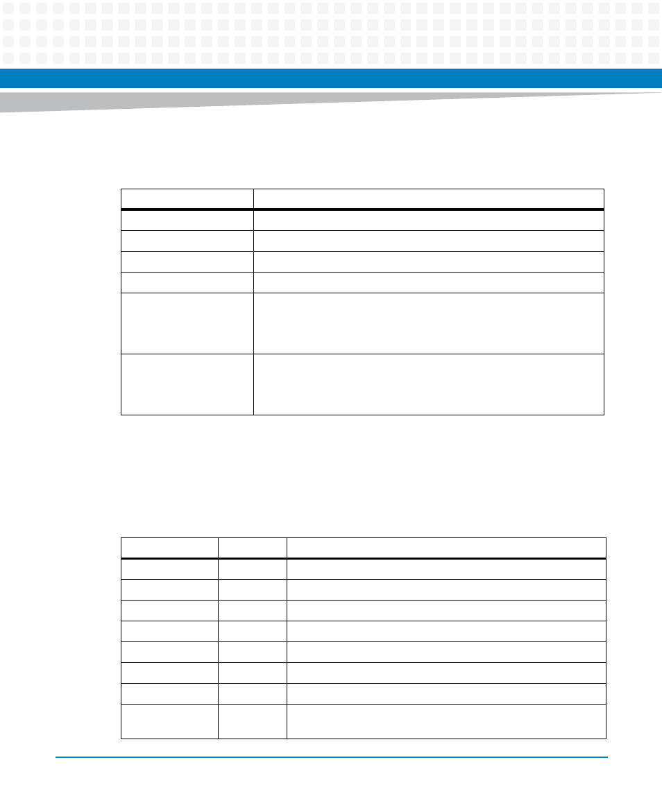
The following table provides an overview of the CPLD registers. For more details, refer to
Registers Detailed Description
.
Table 8-2 Register Access Type
Access
Description
r
Read only
w
Write only
r/w
Read and write
r/w1c
Read and write-1-to-clear, write 0 has no effect
SPI:
The prefix "SPI:" signals that the access is restricted to the IPMC SPI
interface.
E. g.: SPI: r/w means that the register bit is read/writable from the IPMC
SPI interface
SPP:
The prefix "SPP:" signals that the access is restricted to the FPGA SPI
interface.
E. g.: SPP: r/w means that the register bit is read/writable from the CPLD
SPI interface
Table 8-3 CPLD Register Overview
CPLD Address
Type
Description
0x00
r
CPLD Code Version Register
0x01
SPP: r/w
JTAG Update Register
0x02
r
Status Debug Switches, DMC Base ID Register
0x03
r
Status DMC 1 ID and DMC 2 ID Register
0x04
r
GPP Status Signals Part 1Register
0x05
r
GPP Status Signals Part 2Register
0x06
r
SPP and other Status Signals
0x07
SPI: r/w
SPP: r
Scratch Register