3 logic blocks, 1 telecom clocking, Table 8-170 – Artesyn ATCA-8310 Installation and Use (May 2014) User Manual
Page 352: Terminal server spi control register, Cpld and fpga
CPLD and FPGA
ATCA-8310 Installation and Use (6806800M72E)
352
8.2.2.3.42 Terminal Server SPI Control Register
8.2.3
Logic Blocks
8.2.3.1
Telecom Clocking
Clock supervision of all telecom clocks to or from Glue FPGA.
CGM/LCCB Switch over
166 Hz Extended Super Frame clock Generation. The 8 kHz Frame clock is divided by 48.
Phase shift is configurable via SW in 125 us steps.
The SPP should keep the GPP in reset when updating a GPP Boot SPI flash.
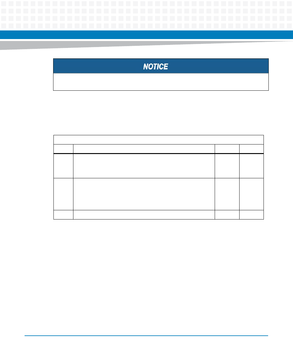
Table 8-170 Terminal Server SPI Control Register
Address: 0xE0
Bit Description
Default
Access
0
Terminal Server SPI Select control:
0: disabled. Select Signal is feed thru
1: enabled. Select Signal controlled by bit 1
0
SPP: r/w
1
Terminal Server SPI Select output:
0: drive TS_SPI_SS_ low
1: drive TS_SPI_SS_ high
Note: Register bit has no effect when bit 0 not set.
0
SPP: r/w
7:2
Reserved
0
r