Table 8-46, Logical device 0x74 reserved register, Table 8-47 – Artesyn ATCA-8310 Installation and Use (May 2014) User Manual
Page 275: Logical device 0x75 reserved register, Table 8-48, Cpld and fpga
CPLD and FPGA
ATCA-8310 Installation and Use (6806800M72E)
275
8.2.2.1.5 GPP COM 1 and COM 2 Register Map
The LPC IO Base addresses BASE1 for COM 1 and BASE2 for COM 2 are set up during Super IO
configuration. See
Chapter 8, Super IO Configuration Registers, on page 268
for more
information.
8.2.2.1.6 GPP UART Register Overview
The UART units are mapped via Super IO (LPC bus). See
GPP COM 1 and COM 2 Register Map
.
Table "GPP UART Register Overview" on page 276
shows the registers and their addresses as
offsets of a base address for one of the two UART units.
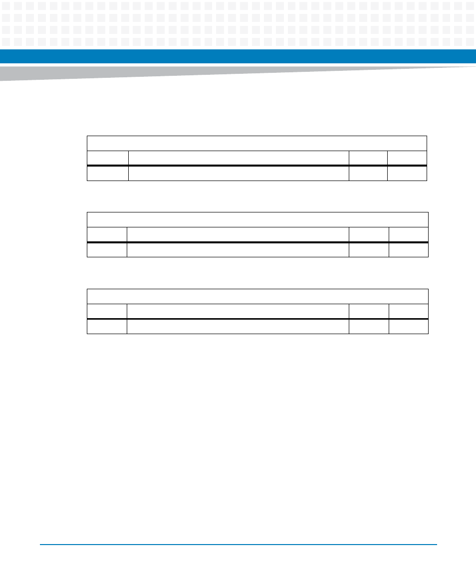
Table 8-46 Logical Device 0x74 Reserved Register
Index Address: 0x74
Bit
Description
Default
Access
7.0
Reserved
0x04
GPP: r
Table 8-47 Logical Device 0x75 Reserved Register
Index Address: 0x75
Bit
Description
Default
Access
7.0
Reserved
0x04
GPP: r
Table 8-48 Logical Device 0x75 Reserved Register
Index Address: 0xF0
Bit
Description
Default
Access
7.0
Reserved
0
GPP: r