Table 8-34, Global configuration register summary, Table 8-35 – Artesyn ATCA-8310 Installation and Use (May 2014) User Manual
Page 270: Super io logical device number register, Table 8-36, Super io device identification register, Cpld and fpga
CPLD and FPGA
ATCA-8310 Installation and Use (6806800M72E)
270
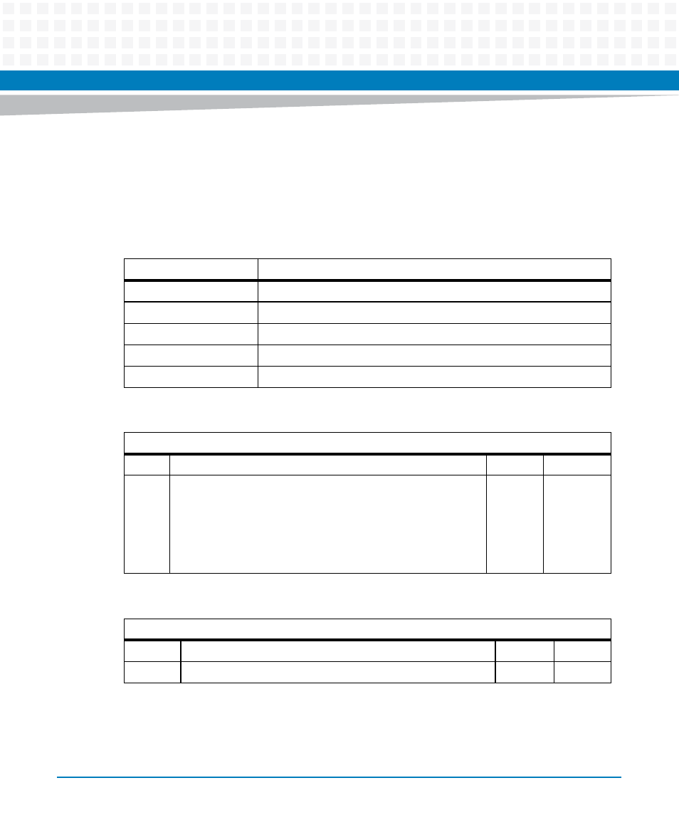
The Super IO Global Registers lie in the address range 0x00-0x2F. All eight bits of the ADDRESS
Port are used for register selection. All unimplemented registers and bits ignore writes and
return zero when read. The INDEX PORT is used to select a configuration register in the chip.
The DATA PORT is then used to access the selected register. These registers are accessible only
in the Configuration Mode.r
Table 8-34 Global Configuration Register Summary
Index Address
Description
0x07
Super IO Logical Device Number
0x20
Super IO Device ID
0x21
Super IO Device Revision
0x28
Super IO LPC Control
0x29
Super IO SERIRQ and Pre-divide Control
Table 8-35 Super IO Logical Device Number Register
Index Address: 0x07
Bit
Description
Default
Access
7:0
Logical Device Number:0x04: Logical Device 4 (COM 1Serial Port
1)
0x05: Logical Device 5 (COM 2 Serial Port 2)
A write to this register selects the current logical device. This
allows access to the control and configuration registers for each
logical device.
0
GPP: r/w
Table 8-36 Super IO Device Identification Register
Index Address: 0x20
Bit
Description
Default
Access
7:0
Device ID
0
GPP: r