Table 8-97, Gpp mailbox output registers, Table 8-98 – Artesyn ATCA-8310 Installation and Use (May 2014) User Manual
Page 315: Spp mailbox output registers, Table 8-99, Gpp mailbox input registers, Table 8-100, Spp mailbox input registers, Cpld and fpga, 19 mailbox registers
CPLD and FPGA
ATCA-8310 Installation and Use (6806800M72E)
315
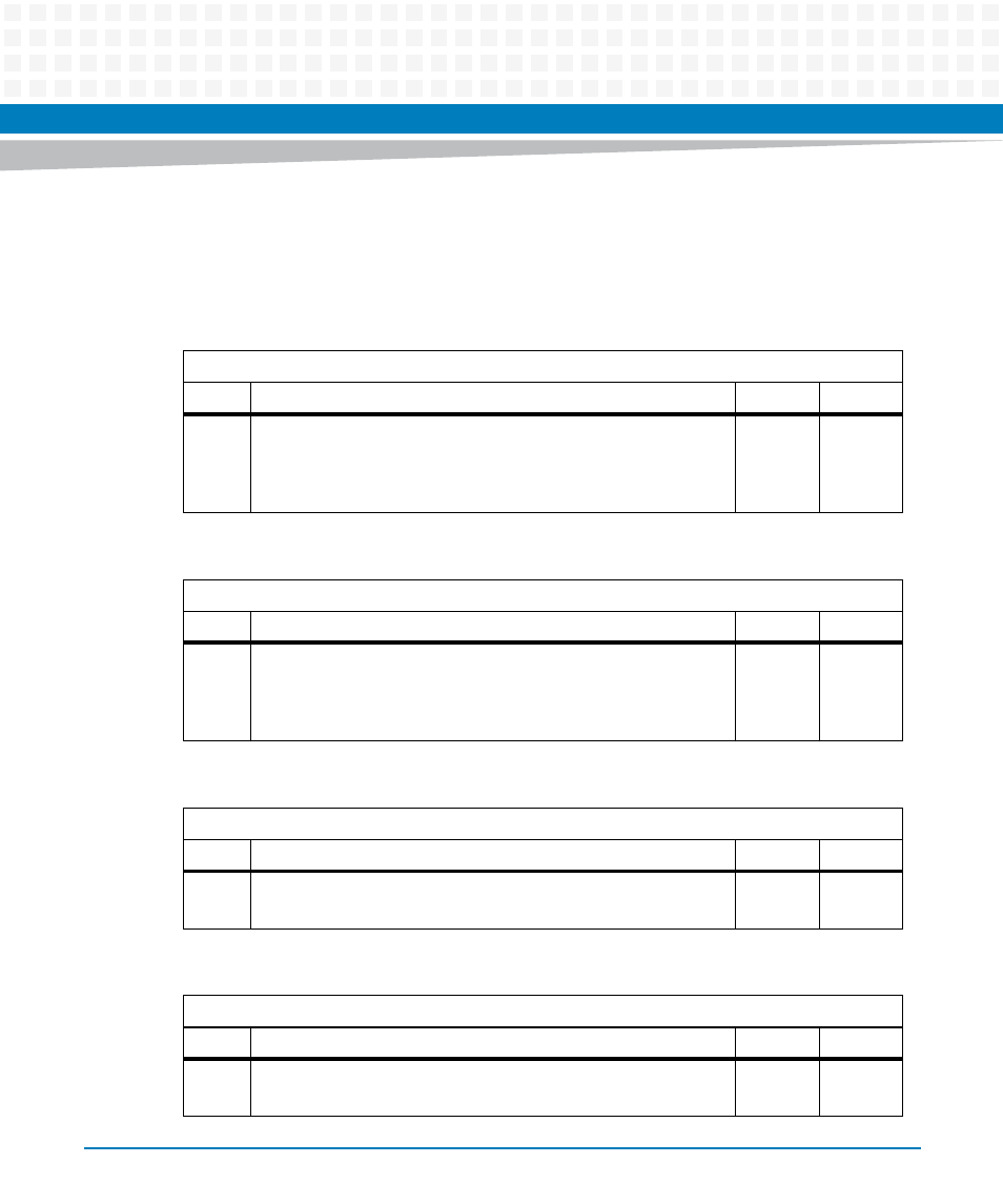
8.2.2.3.19 Mailbox Registers
GPP and SPP have 4 Mailbox registers. Each for Mailbox has a Mailbox output register and a
Mailbox input register.
Table 8-97 GPP Mailbox Output Registers
Address: 0x40, 0x42, 0x44, 0x46
Bit Description
Default
Access
7:0
GPP Mailbox Output Register. 1, 2, 3 and 4:
A write access to the register triggers the corresponding interrupt
on the SPP side and the value can be read on the corresponding
SPP Mailbox Input Register.
0
GPP: r/w
Table 8-98 SPP Mailbox Output Registers
Address: 0x40, 0x42, 0x44, 0x46
Bit Description
Default
Access
7:0
SPP Mailbox Output Register. 1, 2, 3 and 4:
A write access to the register triggers the corresponding interrupt
on the GPP side and the value can be read on the corresponding
GPP Mailbox Input Register.
0
SPP: r/w
Table 8-99 GPP Mailbox Input Registers
Address: 0x41, 0x43, 0x45, 0x47
Bit Description
Default
Access
7:0
GPP Mailbox Input Register. 1, 2, 3 and 4:
Value of the corresponding SPP Mailbox Output Register.
0
GPP: r
Table 8-100 SPP Mailbox Input Registers
Address: 0x41, 0x43, 0x45, 0x47
Bit Description
Default
Access
7:0
SPP Mailbox Input Register. 1, 2, 3 and 4:
Value of the corresponding SPP Mailbox Output Register.
0
SPP: r