Table 8-118, Telecom clock monitor frequency register, Table 8-119 – Artesyn ATCA-8310 Installation and Use (May 2014) User Manual
Page 323: Telecom clock monitor lower limit register, Table 8-120, Telecom clock monitor upper limit register, Table 8-121, Test control and status register, Cpld and fpga, 26 test control and status register
CPLD and FPGA
ATCA-8310 Installation and Use (6806800M72E)
323
8.2.2.3.26 Test Control and Status Register
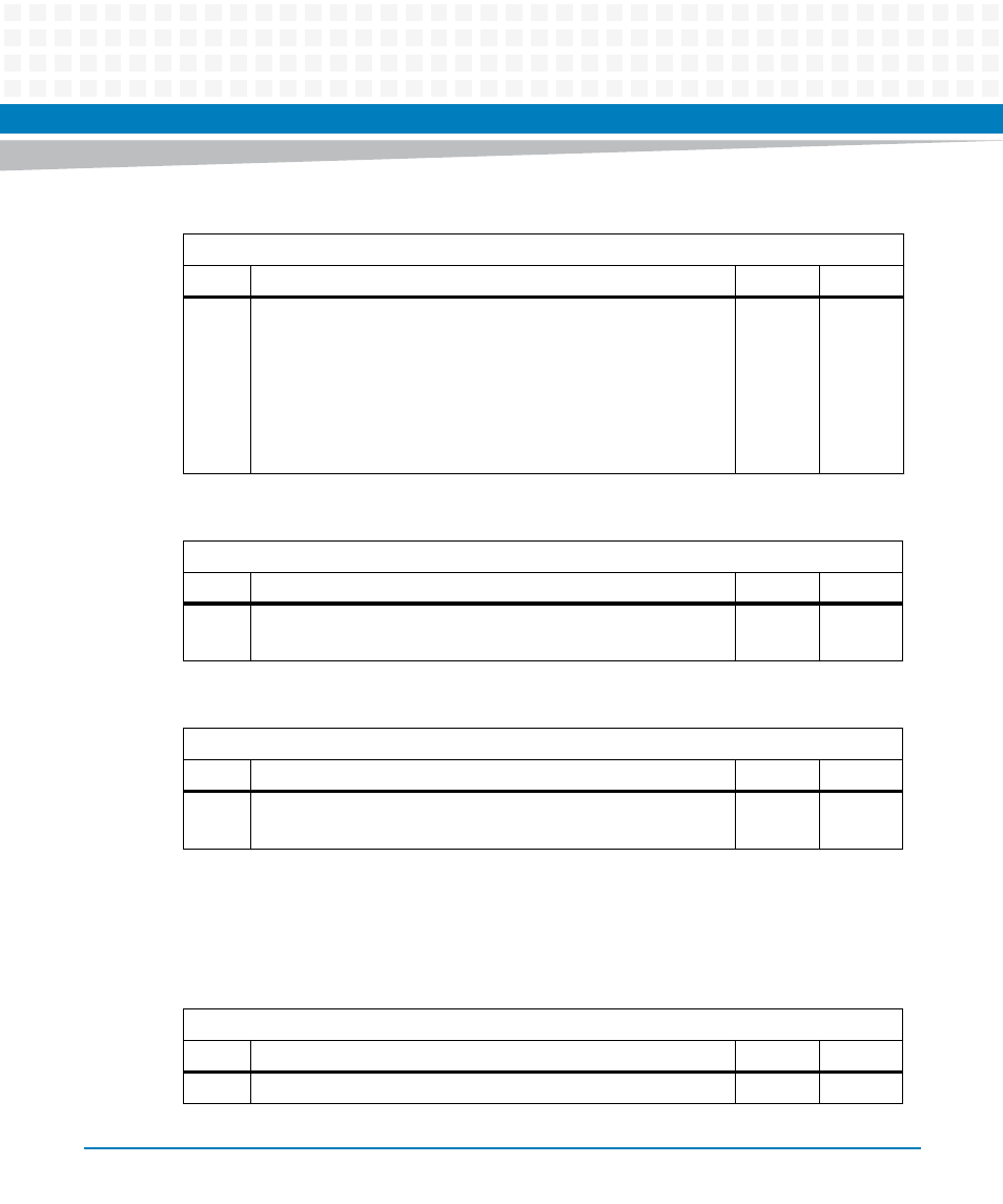
Table 8-118 Telecom Clock Monitor Frequency Register
Address: 0x6A - 0x6B
Bit
Description
Default
Access
15:0
Number of rising clock edges of supervised Telecom Clock during
selected time base.
0: No clock edge sampled. Clock to slow for time base
1 - 65534: Number of sampled clocks during timer base.
65535: Overflow. Clock to fast for time base.
Note: Only valid when corresponding bit in Telecom Clock Monitor
Status Register is set.
0
SPP: r
Table 8-119 Telecom Clock Monitor Lower Limit Register
Address: 0x6C- 0x6D
Bit
Description
Default
Access
15:0
Lower Limit for supervised Telecom Clock:
Used by Telecom Clock Monitor Out of Range Register.
0
SPP: r/w
Table 8-120 Telecom Clock Monitor Upper Limit Register
Address: 0x6E- 0x6F
Bit
Description
Default
Access
15:0
Upper Limit for supervised Telecom Clock:
Used by Telecom Clock Monitor Out of Range Register.
0
SPP: r/w
Table 8-121 Test Control and Status Register
Address: 0x70
Bit Description
Default
Access
0
Test Mode. Only used for simulation.
SPP:0
SPP: r/w