2 glue logic fpga register mapping, Table 8-62, Divisor latch lsb register (dll), if dlab=1 – Artesyn ATCA-8310 Installation and Use (May 2014) User Manual
Page 291: Table 8-63, Divisor latch msb register (dlm), if dlab=1, Cpld and fpga
CPLD and FPGA
ATCA-8310 Installation and Use (6806800M72E)
291
A Divisor value of 0 in the Divisor Latch Register is not allowed.
8.2.2.2
Glue Logic FPGA Register Mapping
8.2.2.2.1 SPP Local Bus Register Map
The SPP set up an IO address range of 256 bytes and uses the chip select signal SPP_LCS_[3].
The upper 128 bytes are only accessed by the SPP. See
Table "Glue FPGA Register Overview" on
8.2.2.2.2 LPC I/O Register Map
The FPGA registers may be accessed via LPC I/O cycles in the I/O address range REGISTERS. See
Table "Glue FPGA Register Overview" on page 292
. For a LPC register access use the base
address 0x600 and add the Address Offset. An LPC I/O write access to an address not listed in
this table or not marked with an "X" in the LPC I/O column is ignored. A corresponding read
access delivers always zero.
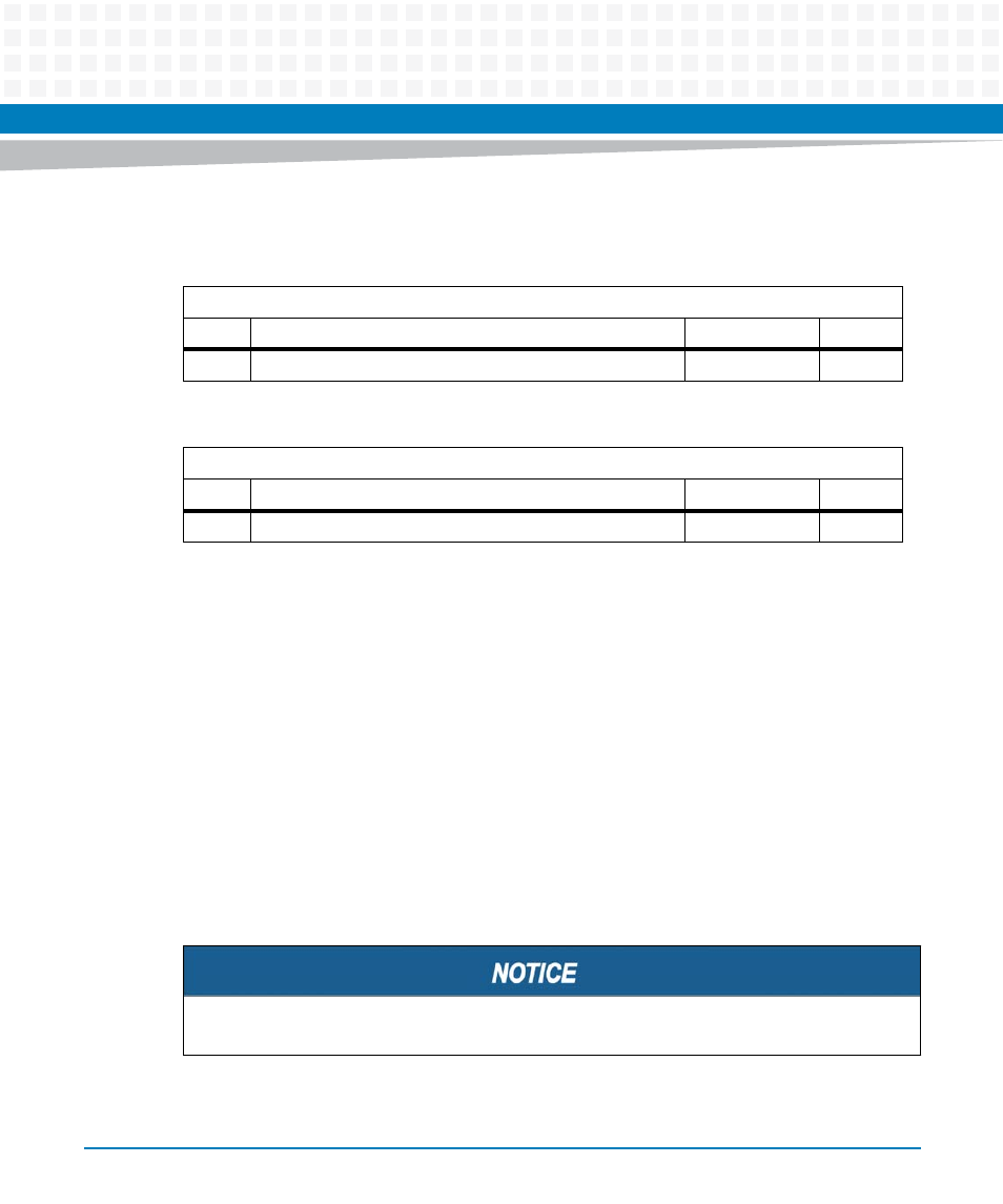
Table 8-62 Divisor Latch LSB Register (DLL), if DLAB=1
IO Address: Base
Bit Description
Default
Access
7:0
Divisor Latch LSB (DLL)
PWR_GOOD: 0.
GPP: r/w
Table 8-63 Divisor Latch MSB Register (DLM), if DLAB=1
IO Address: Base
Bit Description
Default
Access
7:0
Divisor Latch MSB (DLM)
PWR_GOOD: 0.
GPP: r/w
Note: LPC I/O Address = 0x600 + Address Offset