Cpld and fpga – Artesyn ATCA-8310 Installation and Use (May 2014) User Manual
Page 383
CPLD and FPGA
ATCA-8310 Installation and Use (6806800M72E)
383
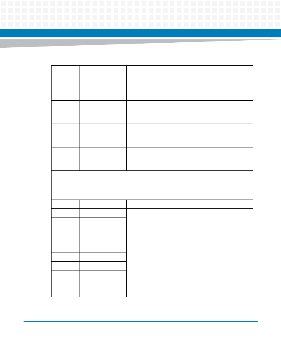
0xE0
FltInsrtReg
Fault Insertion Register (32bit ) [Hw: syn, WAck1, RAck1, WTP
]
Allows simulating several faults initiated not by the original
source but by the host SW for test purposes
0xE4
ScratchPadReg
ScratchPad Register (8bit) [Hw: syn, WAck1, RAck1]
Register memory without any control or status function
0xE8
TestModeCtrlReg
Test Mode Control Register (8bit ) [Hw: asyn, WAck3, RAck3]
Register to control testmodes
0xEC
TestReadValReg
Test Read Val Register (32bit ) [Hw: syn , WAck1 , RAck1]
Register to read data for Hw test purposes
I2C interface to Dsps (I2CIfToDsp) [Hw: Cy0]
The Dsps 0...9 can be accessed via I2c bus through this registers with a simple bit bang interface.
Access via SPI- bus from GlueFpga (occupies 256 Byte address area), hereof assigned to this block:
F0...FB
Address
Acronym
Description
0xF0
I2CBitBang0
I2C Bit Bang Register (8bit ) [Hw: syn , WAck1 , RAck1]
Allows to control and to read the status of an I2C bus to the
respective DSP. I2CBitBang0 Register is connected to Dsp0,
I2CBitBang1 Register is connected to Dsp1 and so on.
0xF1
I2CBitBang1
0xF2
I2CBitBang2
0xF3
I2CBitBang3
0xF4
I2CBitBang4
0xF5
I2CBitBang5
0xF6
I2CBitBang6
0xF7
I2CBitBang7
0xF8
I2CBitBang8
0xF9
I2CBitBang9
Table 8-174 Logic DSP FPGA Register Overview (continued)