1 register decoding, Table 8-28, Byte register layout – Artesyn ATCA-8310 Installation and Use (May 2014) User Manual
Page 265: Table 8-29, Word register layout, Cpld and fpga
CPLD and FPGA
ATCA-8310 Installation and Use (6806800M72E)
265
8.2.2.1
Register Decoding
The Glue Logic FPGA registers may be accessed from the SPP, the GPP or the IPMC. The GPP
uses the GPP LPC bus interface. The IPMC uses the IPMC SPI Slave interface. The SPP uses the
Local Bus Interface.
8.2.2.1.1 SPP Local Bus Decoding
The SPP uses the Local Bus Interface to access Glue Logic FPGA Registers. For Glue Logic FPGA
register access chip select SPP_LCS_[3] is used.
SPP Local Bus to IPMC LPC Bridge
Any SPP access to a KCS register is forwarded to IPMC LPC Host Interface with the
translated IO address 0xCA2 or 0xCA3.
IPMC:
The prefix "IPMC:" signals that the access is restricted to the IPMC SPI
interface. IPMC accesses are forwarded thru the CPLD IPMC SPI
interface. E. g.: IPMC: r/w means that the register bit is read/writable
from the IPMC SPI interface.
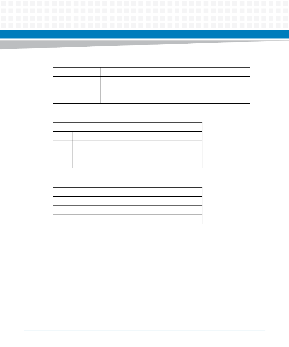
Table 8-28 Byte Register Layout
Address:
Bit Description
0
Least significant Bit
6:1
Group of bits. Lower significant bit is on the right position.
7
Most significant Bit
Table 8-29 Word Register Layout
Address:
Bit Description
7:0
Byte Content of
15:8
Byte content of
Table 8-27 Register Access Type (continued)
Access
Description